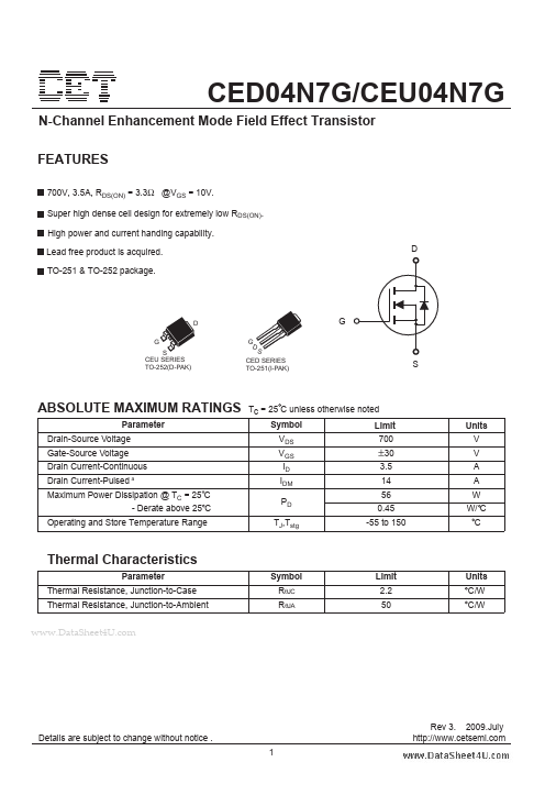
CED04N7G/CEU04N7G
Electrical Characteristics Tc = 25 C unless otherwise noted
Parameter
Symbol
Test Condition
Off Characteristics
Drain-Source Breakdown Voltage
Zero Gate Voltage Drain Current
Gate Body Leakage Current, Forward
Gate Body Leakage Current, Reverse
On Characteristics b
BVDSS
IDSS
IGSSF
IGSSR
VGS = 0V, ID = 250µA
VDS = 700V, VGS = 0V
VGS = 30V, VDS = 0V
VGS = -30V, VDS = 0V
Gate Threshold Voltage
Static Drain-Source
On-Resistance
VGS(th)
RDS(on)
VGS = VDS, ID = 250µA
VGS = 10V, ID = 1.8A
Dynamic Characteristics c
Forward Transconductance
Input Capacitance
Output Capacitance
Reverse Transfer Capacitance
Switching Characteristics c
gFS
Ciss
Coss
Crss
VDS = 40V, ID = 1A
VDS = 25V, VGS = 0V,
f = 1.0 MHz
Turn-On Delay Time
Turn-On Rise Time
Turn-Off Delay Time
td(on)
tr
td(off)
VDD = 300V, ID = 4A,
VGS = 10V, RGEN = 25Ω
Turn-Off Fall Time
tf
Total Gate Charge
Gate-Source Charge
Gate-Drain Charge
Qg
Qgs
VDS = 480V, ID = 4A,
VGS = 10V
Qgd
Drain-Source Diode Characteristics and Maximun Ratings
Drain-Source Diode Forward Current
Drain-Source Diode Forward Voltage b
IS
VSD
VGS = 0V, IS = 3.5A
Notes :
a.Repetitive Rating : Pulse width limited by maximum junction temperature.
b.Device Mounted on FR4 Board, t < 10 sec.
c.Pulse Test : Pulse Width < 300µs, Duty Cycle < 2%.
d.Guaranteed by design, not subject to production testing.
Min
700
2
Typ
2.5
2
595
80
20
18
17
40.5
19
14
3
6
Max Units
25
100
-100
V
µA
nA
nA
4V
3.3 Ω
S
pF
pF
pF
36 ns
34 ns
81 ns
38 ns
18.2 nC
nC
nC
3.5 A
1.5 V
4
www.DataSheet4U.com
2