Datasheet Summary
N-Channel Enhancement Mode Field Effect Transistor Features
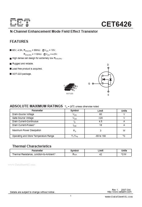
60V, 4.5A, RDS(ON) = 90mΩ @VGS = 10V. RDS(ON) = 110mΩ @VGS = 4.5V. High dense cell design for extremely low RDS(ON). Rugged and reliable. Lead free product is acquired. SOT-223 package. D
D G SOT-223...