Datasheet4U.com
🌙
CET3252 Datasheet | Chino-Excel Technology
Part:
CET3252
Description:
N-Channel MOSFET
Category:
MOSFET
Manufacturer:
Chino-Excel Technology
Size:
415.97 KB
CET3252 Datasheet (PDF) Download
Chino-Excel Technology
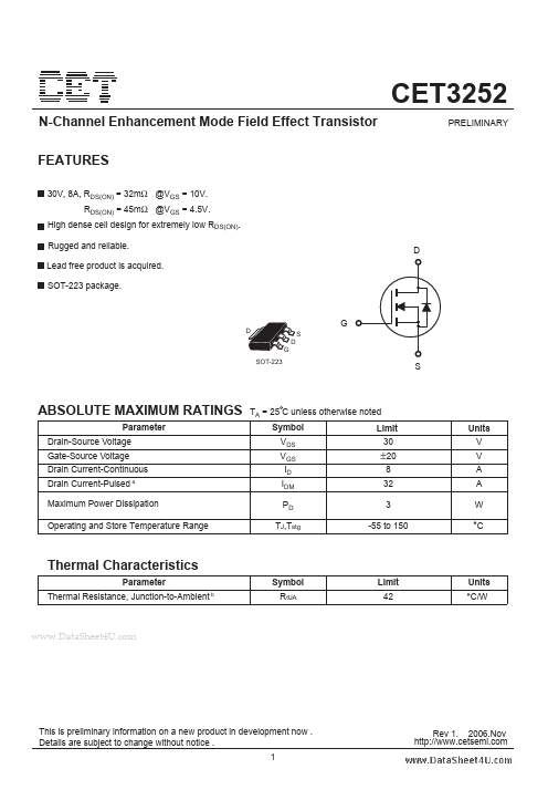
CET3252
Key Features
RDS(ON) = 45mΩ @VGS = 4.5V
High dense cell design for extremely low RDS(ON)
Rugged and reliable
Lead free product is acquired
D PRELIMINARY D G SOT-223 D S G S
×
Close