CS5208-1
CS5208-1 is 8A LDO 3-Pin Adjustable Linear Regulator manufactured by Cherry Semiconductor Corporation.
Description
The CS5208-1 linear regulator provides 8A at adjustable voltages from 1.25V to 4.5V. This adjustable device requires two external resistors to set the output voltage and provide the minimum load current for proper regulation. This regulator is intended for use as a post regulator and microprocessor supply. The fast loop response and low dropout voltage make this regulator ideal for applications where low voltage operation and good transient response are important. The circuit is designed to operate with dropout voltages as low as 1.0V at 8A. The regulator is protected against overload conditions with overcurrent and thermal shutdown protection circuitry. The regulator is available in a TO-220 package.
Features s 1.25V to 4.5V VOUT at 8A s Dropout Voltage < 1.0V @ 8A s 1.5% Trimmed Reference s Fast Transient Response s Thermal Shutdown s Current Limit s Short Circuit Protection
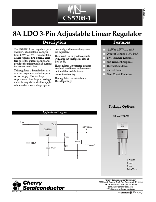
Package Options
Applications Diagram 3 Lead TO-220
5.0V VIN VOUT 3.3V @ 8A
Adj 124 100m F 0.1m F 200 Load 300m F
1. Adjust 2. VOUT 3. VIN Tab = VOUT
Cherry Semiconductor Corporation 2000 South County Trail, East Greenwich, RI 02818 Tel: (401)885-3600 Fax: (401)885-5786 Email: info@cherry-semi. Web Site: .cherry-semi.
Rev. 6/11/97
¨ pany
Absolute Maximum Ratings Input Voltage 6V Operating Junction Temperature Range 0¡C ² TJ ² 150¡C Storage Temperature Range -65¡C to +150¡C Lead Temperature Soldering: Wave Solder (through hole styles only) 10 sec. max, 260¡C peak ESD Damage Threshold...