The following content is an automatically extracted verbatim text
from the original manufacturer datasheet and is provided for reference purposes only.
View original datasheet text
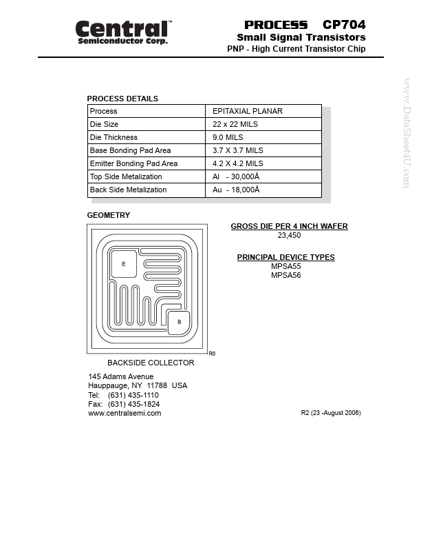
Small Signal Transistors
PROCESS
CP704
PNP - High Current Transistor Chip
www.DataSheet4U.com
PROCESS DETAILS Process Die Size Die Thickness Base Bonding Pad Area Emitter Bonding Pad Area Top Side Metalization Back Side Metalization GEOMETRY GROSS DIE PER 4 INCH WAFER 23,450 PRINCIPAL DEVICE TYPES MPSA55 MPSA56 EPITAXIAL PLANAR 22 x 22 MILS 9.0 MILS 3.7 X 3.7 MILS 4.2 X 4.2 MILS Al - 30,000Å Au - 18,000Å
BACKSIDE COLLECTOR 145 Adams Avenue Hauppauge, NY 11788 USA Tel: (631) 435-1110 Fax: (631) 435-1824 www.centralsemi.com
R2 (23 -August 2006)
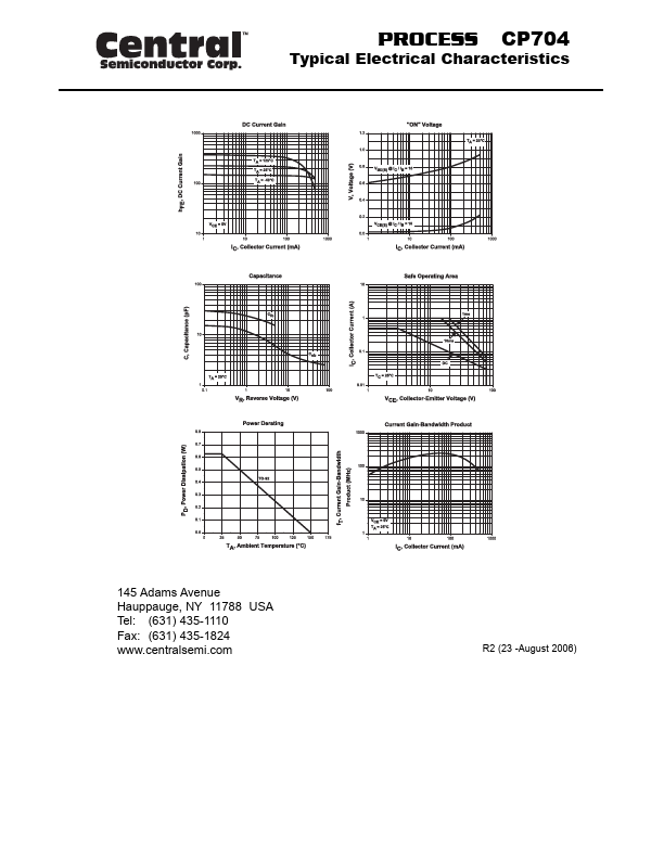
Typical Electrical Characteristics
PROCESS
CP704
145 Adams Avenue Hauppauge, NY 11788 USA Tel: (631) 435-1110 Fax: (631) 435-1824 www.centralsemi.
 CP704 Datasheet