The following content is an automatically extracted verbatim text
from the original manufacturer datasheet and is provided for reference purposes only.
View original datasheet text
N-Channel JFET General Purpose Amplifier
CORPORATION
2N4117 – 2N4119 / 2N4117A – 2N4119A PN4117 – PN4119 / PN4117A – PN4119A / SST4117 – SST4119
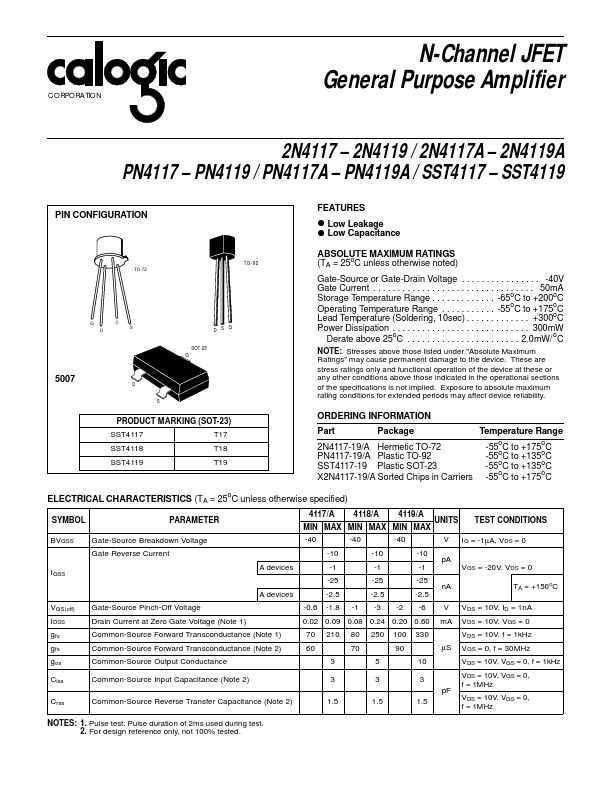
PIN CONFIGURATION FEATURES Leakage • Low • Low Capacitance
TO - 92
TO-72
ABSOLUTE MAXIMUM RATINGS (TA = 25oC unless otherwise noted) Gate-Source or Gate-Drain Voltage . . . . . . . . . . . . . . . . -40V Gate Current . . . . . . . . . . . . . . . . . . . . . . . . . . . . . . . . . 50mA Storage Temperature Range . . . . . . . . . . . . . -65oC to +200oC Operating Temperature Range . . . . . . . . . . . -55oC to +175oC Lead Temperature (Soldering, 10sec) . . . . . . . . . . . . . +300oC Power Dissipation . . . . . . . . . . . . . . . . . . . . . . . . . . . . 300mW Derate above 25oC . . . . . . . . . . . . . . . . . . . . . . . 2.
 PN4119 Datasheet