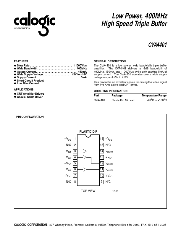
CVA4401
CORPORATION
ABSOLUTE MAXIMUM RATINGS (Note 1)
Supply Voltage. . . . . . . . . . . . . . . . . . . . . . . . . . . . . . . . . ±20V
Input Voltage . . . . . . . . . . . . . . . . . . . . . . . . . . . . . . ±Vsupply
Storage Temperature Range . . . . . . . . . . . . -65oC to +150oC
Lead Temperature
(Soldering 10 seconds) . . . . . . . . . . . . . . . . . . . . . . 260oC
Power Dissipation . . . . . . . . . . . . . . . . . . . . . . . . . . . (Note 4)
ESD Tolerance (Note 3). . . . . . . . . . . . . . . . . . . . . . . ±2000V
Thermal Resistance (θJA)
N Package . . . . . . . . . . . . . . . . . . . . . . . . . . . . . . .
95oC/W
Thermal Resistance (θJC)
N Package . . . . . . . . . . . . . . . . . . . . . . . . . . . . . . . 50oC/W
Maximum Junction Temperature . . . . . . . . . . . . . . . . . . 150oC
DC ELECTRICAL CHARACTERISTICS
The following specifications apply for Supply Voltage = ±12V, VCM = 0, RL ≥ 100KΩ and RS = 50Ω unless otherwise noted.
SYMBOL
CHARACTERISTICS TYP
Limit
(Note 5)
UNITS
CONDITIONS
AV1
Voltage Gain 1
0.99 0.96
RL = ∞, VIN = ±10V
V/V Min
AV2
Voltage Gain 2
0.95 0.90
RL = 100Ω, VIN = ±10V
VOS Offset Voltage
10 50 mV Max RL = ∞
IB Input Bias Current 1 25 µA Max RL = ∞
RIN
Input Resistance
0.5
MΩ RL = 100Ω
CIN
Input Capacitance
3.5
pF
RO Output Resistance 3 10 Ω Max RL = 100Ω, VIN = ±2V
IS
Supply Current
5 7.5 mA Max RL = ∞
VO Output Swing
8 8 ±V Min RL = 100Ω, VIN = ±10V
IOUT
Output Current
150 100
mA VIN = 10V
AC ELECTRICAL CHARACTERISTICS
The following specifications apply for Supply Voltage = ±12V, VCM = 0, RL ≥ 100KΩ and RS = 50Ω unless otherwise noted.
SYMBOL
CHARACTERISTICS TYP
Limit
(Note 5)
UNITS
CONDITIONS
SR1
SSBW
PBW
tr, tf
t pd
Slew Rate 1
11000
Small Signal Bandwidth 400
Power Bandwidth
Rise Time
Fall Time
Propagation Delay Time
100
1.2
2.0
8000
200
1.7
V/µs
MHz
ns
ns
VIN = ±10V, RL = 100Ω (Note 2)
VIN = ±100mVPP, RL = 100Ω
CL ≤ 10pF
VIN = ±4V, RL = 100Ω
CL ≤ 10pF
RL = 100Ω, CL ≤ 10pF
VIN = 0.5V
RL = 100Ω, CL ≤ 10pF
VIN = 0.5V
Note 1: Absolute Maximum Ratings indicate limits beyond which damage to the device may occur. DC and AC electrical specifications do not
apply when operating the device beyond its rated operating conditions.
Note 2: Slew rate is measured with 50Ω source impedance at 25oC. Slew rate is measured between VO = +5V and -5V.
Note 3: The test circuit consists of the human body model of 120pF in series with 1500Ω.
Note 4: The maximum power dissipation is a function of TJ(max), θJA and TA. The maximum allowable power dissipation at any ambient
temperature is PD = (TJ(max) - TA)/θJA.
Note 5: Limits are guaranteed by testing, correlation or periodic characterization.
Information furnished by Calogic is believed to be accurate and reliable. However, no responsibility is assumed for its use: nor for any infringement of patents or other
rights of third parties which may result from its use. No license is granted by implication or otherwise under any patent rights of Calogic.
CALOGIC CORPORATION, 237 Whitney Place, Fremont, California 94539, Telephone: 510-656-2900, FAX: 510-651-3025