MTC3586DFA6
Description
RDSON(TYP.) 37mΩ(VGS=2.5V) 115mΩ(VGS=-2.5V) 82mΩ(VGS=1.5V) 280mΩ(VGS=-1.5V)
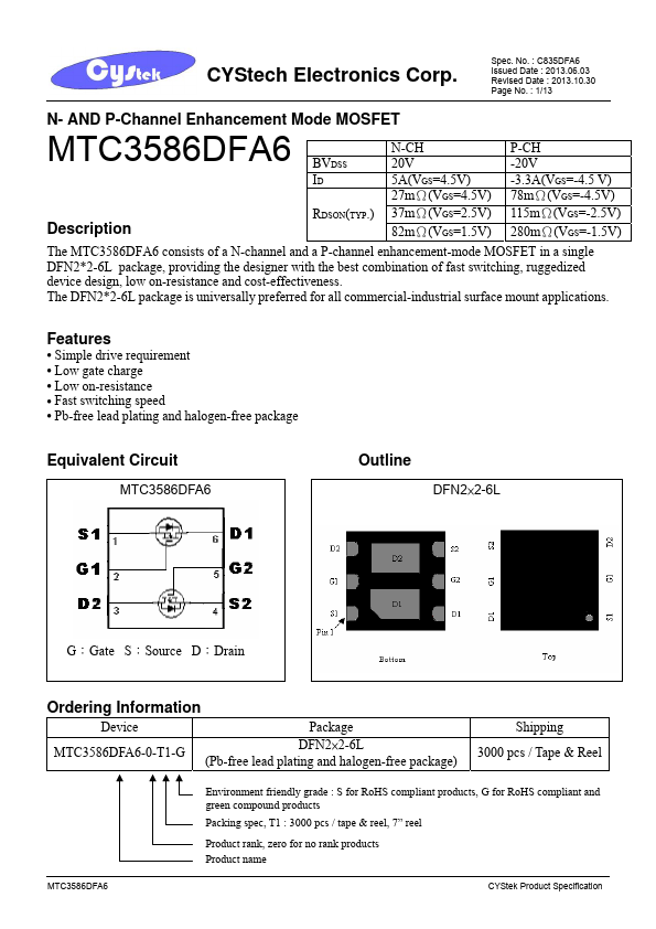
The MTC3586DFA6 consists of a N-channel and a P-channel enhancement-mode MOSFET in a single DFN2- 2-6L package, providing the designer with the best bination of fast switching, ruggedized device design, low on-resistance and cost-effectiveness. The DFN2- 2-6L package is universally preferred for all mercial-industrial surface mount applications.
Features
- Simple drive requirement
- Low gate charge
- Low on-resistance
- Fast switching speed
- Pb-free lead plating and halogen-free package
Equivalent Circuit
Outline
DFN2×2-6L
G:Gate S:Source D:Drain
Ordering Information
Device
Package
MTC358...