The following content is an automatically extracted verbatim text
from the original manufacturer datasheet and is provided for reference purposes only.
View original datasheet text
CYStech Electronics Corp.
20V N-CHANNEL Enhancement Mode MOSFET
MTN2302V3
Spec. No. : C323V3 Issued Date : 2009.01.19 Revised Date : 2010.06.18 Page No. : 1/9
Features
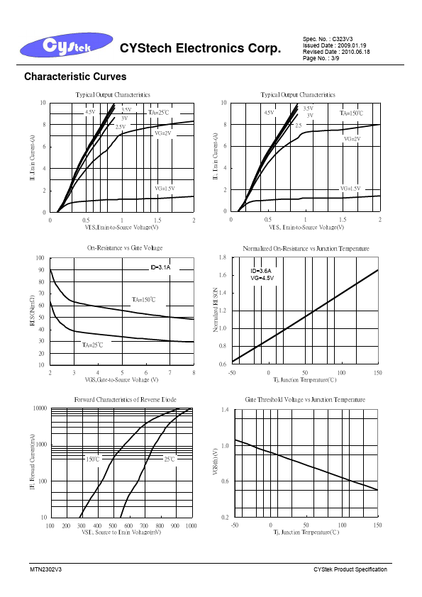
• VDS=20V RDS(ON)=85mΩ(max.)@VGS=4.5V, IDS=3.6A RDS(ON)=115mΩ(max.)@VGS=2.5V, IDS=3.1A
• Simple drive requirement • Small package outline • Capable of 2.5V gate drive • Pb-free package
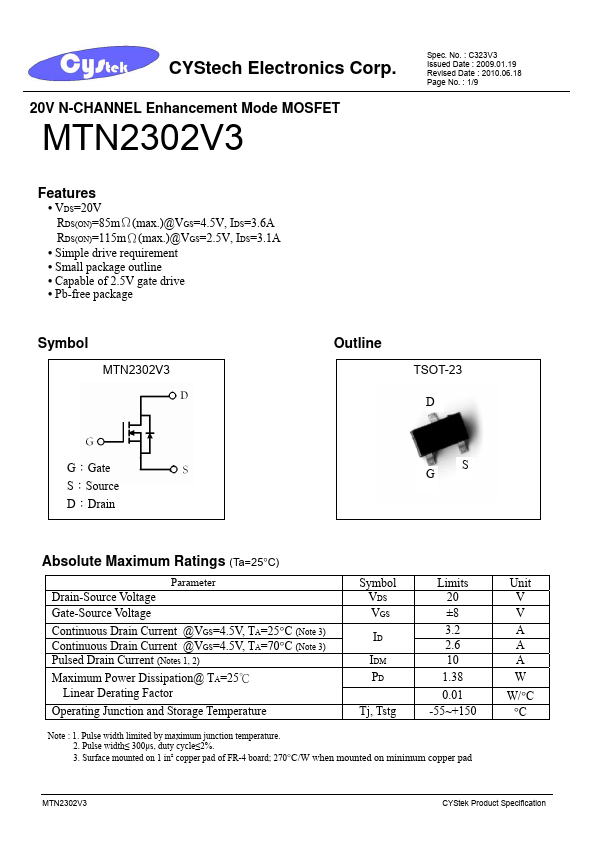
Symbol
MTN2302V3
Outline
TSOT-23 D
G:Gate S:Source D:Drain
GS
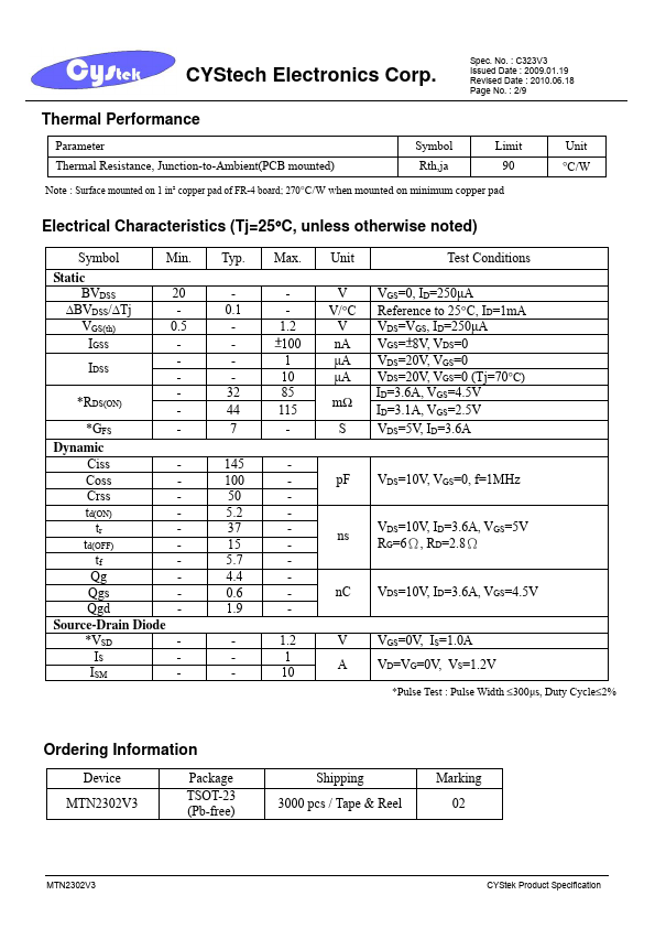
Absolute Maximum Ratings (Ta=25°C)
Parameter
Drain-Source Voltage Gate-Source Voltage Continuous Drain Current @VGS=4.5V, TA=25°C (Note 3) Continuous Drain Current @VGS=4.5V, TA=70°C (Note 3) Pulsed Drain Current (Notes 1, 2)
Maximum Power Dissipation@ TA=25℃ Linear Derating Factor
Operating Junction and Storage Temperature
Symbol VDS VGS
ID IDM PD
Tj, Tstg
Limits 20 ±8 3.
 MTN2302V3 Datasheet