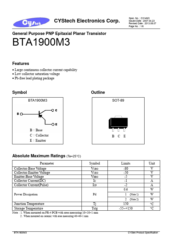
Pb-free lead plating package
Symbol
BTA1900M3
Outline
SOT-89
B:Base C:Collector E:Emitter
BCE
Absolute Maximum Ratings (Ta=25°C)
Parameter
Collector-Base Voltage Collector-Emitter Voltage Emitter-Base Voltage Collector Current(DC) Collector Current(Pulse)
Symbol
VCBO VCEO VEBO
IC ICP
Power Dissipation
Pd
Junction Temperature
Tj
Storage Temperature
Tstg
Note : 1. When mounted.
The following content is an automatically extracted verbatim text
from the original manufacturer datasheet and is provided for reference purposes only.
View original datasheet text
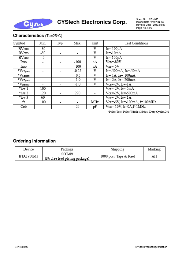
CYStech Electronics Corp.
General Purpose PNP Epitaxial Planar Transistor
BTA1900M3
Spec. No. : C314M3 Issued Date : 2007.04.23 Revised Date : 2013.08.07 Page No. : 1/6
Features
• Large continuous collector current capability • Low collector saturation voltage • Pb-free lead plating package
Symbol
BTA1900M3
Outline
SOT-89
B:Base C:Collector E:Emitter
BCE
Absolute Maximum Ratings (Ta=25°C)
Parameter
Collector-Base Voltage Collector-Emitter Voltage Emitter-Base Voltage Collector Current(DC) Collector Current(Pulse)
Symbol
VCBO VCEO VEBO
IC ICP
Power Dissipation
Pd
Junction Temperature
Tj
Storage Temperature
Tstg
Note : 1. When mounted on FR-4 PCB with area measuring 10×10×1 mm
2 . When mounted on ceramic with area measuring 40×40×1 mm
Limits
-80 -50 -5 -1 -2
0.
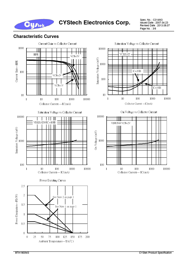
 BTA1900M3 Datasheet