CGHV96100F2
CGHV96100F2 is Input/Output Matched GaN HEMT / Power Amplifer manufactured by Cree.
100 W, 7.9
- 9.6 GHz, 50-ohm, Input/Output Matched GaN HEMT, Power Amplifier
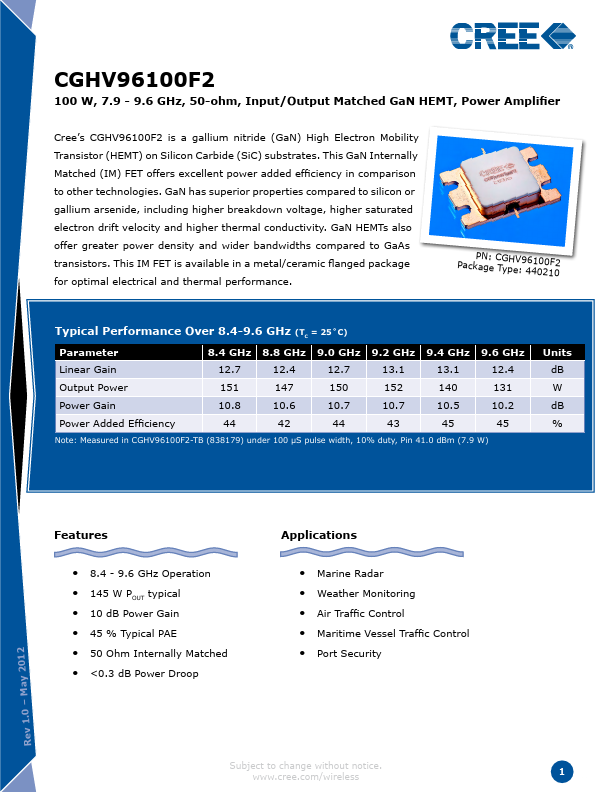
Cree’s CGHV96100F2 is a gallium nitride (GaN) High Electron Mobility Transistor (HEMT) on Silicon Carbide (SiC) substrates. This GaN Internally Matched (IM) FET offers excellent power added efficiency in parison to other technologies. GaN has superior properties pared to silicon or gallium arsenide, including higher breakdown voltage, higher saturated electron drift velocity and higher thermal conductivity. GaN HEMTs also offer greater power density and wider bandwidths pared to GaAs transistors. This IM FET is available in a metal/ceramic flanged package for optimal electrical and thermal...