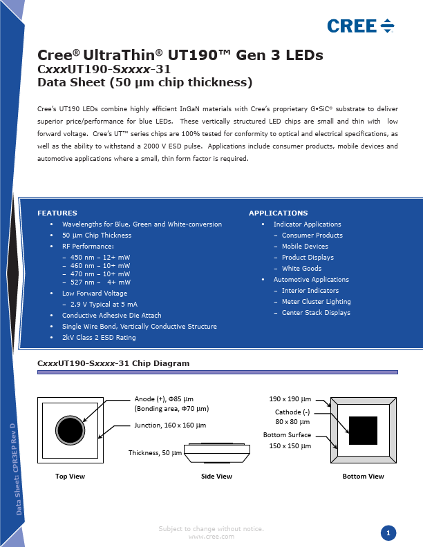
P-N Junction Area (μm) Chip Top Area (μm) Chip Bottom Area (μm) Chip Thickness (μm) Au Bond Pad Diameter (μm) Bonding Area Note 5 Diameter (μm) Au Bond Pad Thickness (μm) Backside Contact Metal Area (μm)
CxxxUT190-Sxxxx-31
Dimension
Tolerance
160 x 160
± 25
190 x 190
± 25
150 x 150
± 25
50
Key Features
Wavelengths for Blue, Green and White-conversion.
50 mm Chip Thickness.
RF Performance:.
450 nm.
12+ mW.
460 nm.
10+ mW.
470 nm.
10+ mW.
527 nm.
4+ mW.
Low Forward Voltage.
2.9 V Typical at 5 mA.
Conductive Adhesive Die Attach.
Single Wire Bond, Vertically Conductive Structure.
2kV Class 2 ESD Rating
CxxxUT190-Sxxxx-31 Chip Diagram.
Full PDF Text Transcription for C460UT190 (Reference)
Note: Below is a high-fidelity text extraction (approx. 800 characters) for
C460UT190. For precise diagrams, and layout, please refer to the original PDF.
Cree® UltraThin® UT190™ Gen 3 LEDs CxxxUT190-Sxxxx-31 Data Sheet (50 µm chip thickness) Cree’s UT190 LEDs combine highly efficient InGaN materials with Cree’s proprietary...
View more extracted text
LEDs combine highly efficient InGaN materials with Cree’s proprietary G•SiC® substrate to deliver superior price/performance for blue LEDs. These vertically structured LED chips are small and thin with low forward voltage. Cree’s UT™ series chips are 100% tested for conformity to optical and electrical specifications, as well as the ability to withstand a 2000 V ESD pulse. Applications include consumer products, mobile devices and automotive applications where a small, thin form factor is required.