The following content is an automatically extracted verbatim text
from the original manufacturer datasheet and is provided for reference purposes only.
View original datasheet text
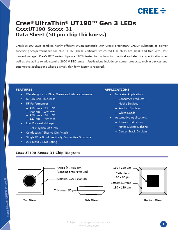
Cree® UltraThin® UT190™ Gen 3 LEDs
CxxxUT190-Sxxxx-31 Data Sheet (50 µm chip thickness)
Cree’s UT190 LEDs combine highly efficient InGaN materials with Cree’s proprietary G•SiC® substrate to deliver superior price/performance for blue LEDs. These vertically structured LED chips are small and thin with low forward voltage. Cree’s UT™ series chips are 100% tested for conformity to optical and electrical specifications, as well as the ability to withstand a 2000 V ESD pulse. Applications include consumer products, mobile devices and automotive applications where a small, thin form factor is required.
 C450UT190 Datasheet