CS10L45CT-A
Key Features
- Low forward voltage drop
- Excellent high temperature stability
- Fast switching capability
- Suffix "G" indicates Halogen-free part, ex.CS10L45CTG-A
- Lead free in pliance with EU RoHS
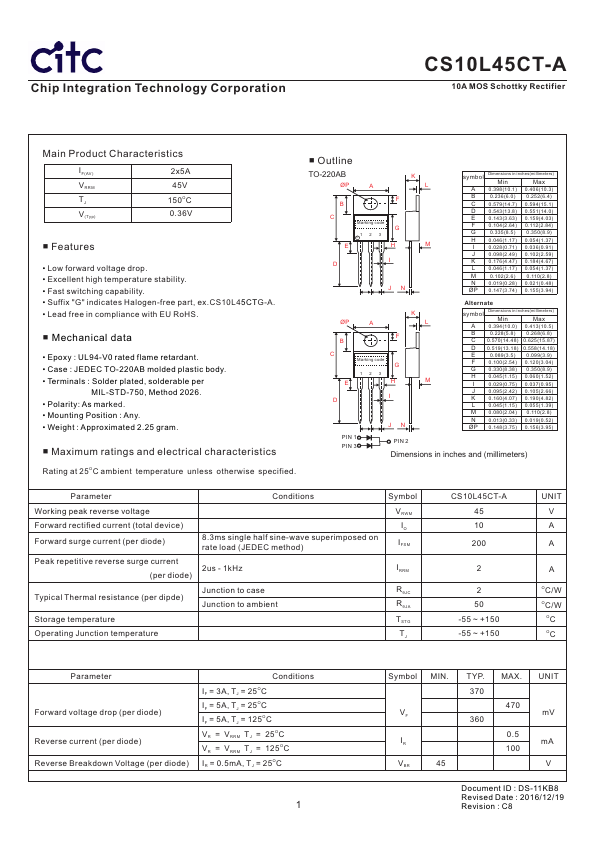
- Mechanical data
- Epoxy : UL94-V0 rated flame retardant
- Case : JEDEC TO-220AB molded plastic body
- Terminals : Solder plated, solderable per MIL-STD-750, Method
- Polarity: As marked