PS5005
PS5005 is Step-up DC/DC Converter manufactured by CHIPLINK.
DESCRIPTION
The PS5005 is a pact, high efficiency, and low voltage step-up DC/DC converter with an Adaptive Current Mode PWM control loop. It prises of an error amplifier, a ramp generator, a PWM parator, a switch pass element and the driver. It provides stable and high efficient operation over a wide range of load currents without external pensation. The below 1V start-up input voltage makes PS5005 suitable for single battery cell applications. The built-in power transistor is able to provide up to 300m A output current while working under Li-Battery Supply. Besides, it provides extra pin to drive external power devices (NMOS or NPN ) in case higher output current is needed. The output voltage is set with two external resistors. The 500KHz high switching rate reduces the size of external ponents. Besides, the 14µA low quiescent current together with high efficiency maintains long battery lifetime.
FEATURES
- -
- -
- -
- - Low Quiescent (Switch-off) Supply Current: 14µA Low Start-up Input Voltage: typical 0.8V High Supply Capability: Deliver 3.3V 100m A with 1Alkaline Cell; 5V 300m A with 1 Li-Cell Zero Shutdown Mode Supply Current High efficiency: 90% Fixed switching frequency: 500KHz Options for internal or external power switches Package type: SOT-26, SOT-89-5
APPLICATIONS
MP3, PDA, Electronic Dictionary, DSC, LCD, RF-Tag, Portable Devices, Wireless Devices, etc.
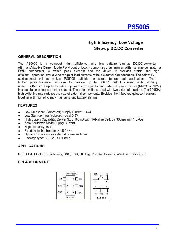
PIN ASSIGNMENT
PIN DESCRIPTION
ORDER INFORMATION
BLOCK DIAGRAM
ABSOLUTE MAXIMUM RATINGS
ELECTRICAL CHARACTERISTICS
TYPICAL APPLICATION CIRCUITS
Note:Cc for better Stability
Extending Output Current
Note:Cc for better Stability
Note:Cc for better Stability
APPLICATION DESIGN GUIDELINES
1) Output Voltage Setting Referring to Typical Application Circuit 1, the output voltage of switching regulator (Vout) is set with following equation: Vout=(1+R1/R2)- Vfb 2) Feedback Loop Design Referring to Typical Application Circuit 1 again, the selection of R1 and R2...