Datasheet Specifications
- Part number
- CEU61A2
- Manufacturer
- CET
- File Size
- 288.98 KB
- Datasheet
- CEU61A2_CET.pdf
- Description
- N-Channel MOSFET
Description
CED61A2/CEU61A2 N-Channel Enhancement Mode Field Effect Transistor .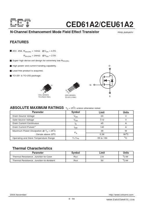
Features
* 20V, 45A, RDS(ON) = 14mΩ @VGS = 4.5V. RDS(ON) = 24mΩ @VGS = 2.5V. Super high dense cell design for extremely low RDS(ON). High power and current handing capability. Lead free product is acquired. TO-251 & TO-252 package. D PRELIMINARY D G S CEU SERIES TO-252(D-PAK) G D G S CED SERIES TO-251(I-PAK)CEU61A2 Distributors
📁 Related Datasheet
📌 All Tags