CEU6060R Description
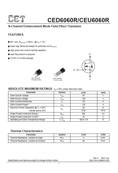
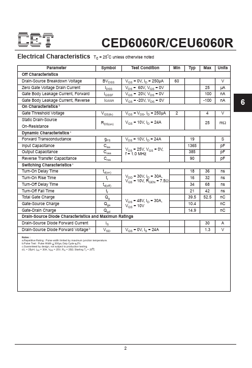
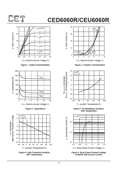
CED6060R/CEU6060R N-Channel Enhancement Mode Field Effect Transistor.
| Part number | CEU6060R |
|---|---|
| Download | CEU6060R Datasheet (PDF) |
| File Size | 375.91 KB |
| Manufacturer | CET |
| Description | N-Channel MOSFET |
|
|
| Part Number | Description |
|---|---|
| CEU6060N | N-Channel MOSFET |
| CEU6030L | N-Channel MOSFET |
| CEU6031L | N-Channel MOSFET |
| CEU6042 | N-Channel MOSFET |
| CEU6056 | N-Channel MOSFET |
CED6060R/CEU6060R N-Channel Enhancement Mode Field Effect Transistor.