Datasheet4U.com
🌙
CEU51A3
CEU5175
CEU51A3 Datasheet | CET
Part:
CEU51A3
Description:
N-Channel MOSFET
Category:
MOSFET
Manufacturer:
CET
Size:
139.75 KB
CEU51A3 Datasheet (PDF) Download
CET
CEU51A3
Key Features
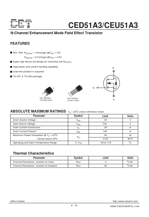
G S CEU SERIES TO-252(D-PAK) G
×
Close