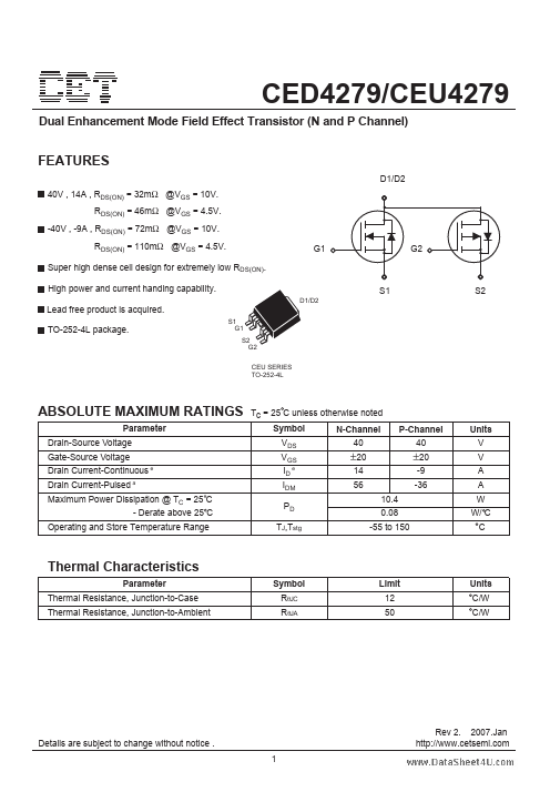
• Part: CEU4279
  • Description: Dual MOSFET
  • Category: MOSFET
  • Manufacturer: CET
  • Size: 678.21 KB
Download CEU4279 Datasheet PDF
CET
CEU4279
CEU4279 is Dual MOSFET manufactured by CET.
Features 40V , 14A , RDS(ON) = 32mΩ @VGS = 10V. RDS(ON) = 46mΩ @VGS = 4.5V. -40V , -9A , RDS(ON) = 72mΩ @VGS = 10V. RDS(ON) = 110mΩ @VGS = 4.5V. Super high dense cell design for extremely low RDS(ON). High power and current handing capability. Lead free product is acquired. TO-252-4L package. S1 G1 S2 G2 CEU SERIES TO-252-4L D1/D2 G1 G2 S1 S2 ABSOLUTE MAXIMUM RATINGS Parameter Drain-Source Voltage Gate-Source Voltage Drain Current-Continuous e Drain Current-Pulsed a Tc = 25 C unless otherwise noted Symbol N-Channel VDS VGS ID e IDM PD TJ,Tstg 40 P-Channel 40 Units V V A A W W/ C C ±20 14 56 10.4 0.08 -55 to 150 ±20 -9 -36 Maximum Power Dissipation @ TC = 25 C - Derate above 25 C Operating and Store Temperature Range Thermal Characteristics Parameter Thermal Resistance, Junction-to-Case Thermal Resistance, Junction-to-Ambient Symbol RθJC RθJA Limit 12 50 Units C/W C/W Details are subject to change without notice . 1 Rev 2. 2007.Jan http://.cetsemi. CED4279/CEU4279 N-Channel Electrical Characteristics Parameter Off Characteristics Drain-Source Breakdown Voltage Zero Gate Voltage Drain Current Gate Body Leakage Current, Forward Gate Body Leakage Current, Reverse On Characteristics Gate Threshold Voltage Static Drain-Source On-Resistance Dynamic Characteristics Input Capacitance Output Capacitance Reverse Transfer Capacitance Switching Characteristics d Turn-On Delay Time Turn-On Rise Time Turn-Off Delay Time Turn-Off Fall Time Total Gate Charge Gate-Source Charge Gate-Drain Charge Drain-Source Diode Forward Current b Drain-Source Diode Forward Voltage c td(on) tr td(off) tf Qg Qgs Qgd IS VSD VGS = 0V, IS = 1A VDS = 20V, ID = 6A, VGS = 4.5V VDD = 20V, ID = 6A, VGS = 10V, RGEN = 3Ω 15 11 18 19 10 3.7 4.2 8 1.2 30 22 36 38 13.3 ns ns ns ns n C n C n C A V d TA = 25 C unless otherwise noted Test Condition VGS = 0V, ID = 250µA VDS = 40V, VGS = 0V VGS = 20V, VDS = 0V VGS = -20V, VDS = 0V VGS = VDS, ID = 250µA VGS = 10V, ID = 8A VGS = 4.5V, ID = 6A VDS = 5V, ID...