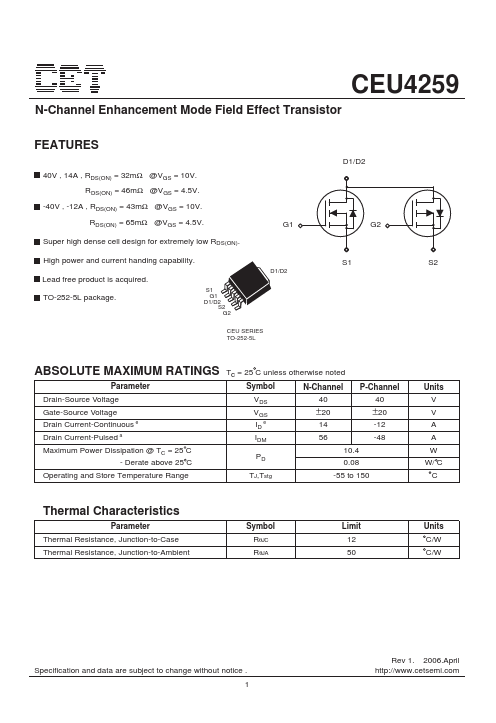
CEU4259
N-Channel Electrical Characteristics TA = 25 C unless otherwise noted
Parameter
Symbol
Test Condition
Min Typ Max Units
Off Characteristics
Drain-Source Breakdown Voltage
Zero Gate Voltage Drain Current
Gate Body Leakage Current, Forward
Gate Body Leakage Current, Reverse
On Characteristics
BVDSS
IDSS
IGSSF
IGSSR
VGS = 0V, ID = 250µA
VDS = 40V, VGS = 0V
VGS = 20V, VDS = 0V
VGS = -20V, VDS = 0V
40
1
100
-100
V
µA
nA
nA
Gate Threshold Voltage
Static Drain-Source
On-Resistance
Dynamic Characteristics d
Forward Transconductance
Input Capacitance
Output Capacitance
Reverse Transfer Capacitance
Switching Characteristics d
VGS(th)
RDS(on)
gFS c
Ciss
Coss
Crss
VGS = VDS, ID = 250µA
VGS = 10V, ID = 7A
VGS = 4.5V, ID = 5A
1
3V
25 32 mΩ
35 46 mΩ
VDS = 10V, ID = 7A
VDS = 20V, VGS = 0V,
f = 1.0 MHz
3
1050
155
95
S
pF
pF
pF
Turn-On Delay Time
Turn-On Rise Time
Turn-Off Delay Time
td(on)
tr
td(off)
VDD = 20V, ID = 6A,
VGS = 10V, RGEN = 3Ω
Turn-Off Fall Time
tf
Total Gate Charge
Gate-Source Charge
Gate-Drain Charge
Qg
Qgs
VDS = 20V, ID = 6A,
VGS = 10V
Qgd
Drain-Source Diode Characteristics and Maximun Ratings
Drain-Source Diode Forward Current b
Drain-Source Diode Forward Voltage c
IS
VSD
VGS = 0V, IS = 1.0A
14 30
10 20
17 35
18 35
20.5 27
3.5
4.0
ns
ns
ns
ns
nC
nC
nC
8A
1.2 V
Notes :
a.Repetitive Rating : Pulse width limited by maximum junction temperature.
b.Surface Mounted on FR4 Board, t < 10 sec.
c.Pulse Test : Pulse Width < 300µs, Duty Cycle < 2%.
d.Guaranteed by design, not subject to production testing.
e.Calculated continuous current based on the maximum allowable junction temperature. Package limitation current=8A.
2