Part number:
CEU3120
Manufacturer:
CET
File Size:
242.36 KB
Description:
N-channel mosfet.
CEU3120 Features
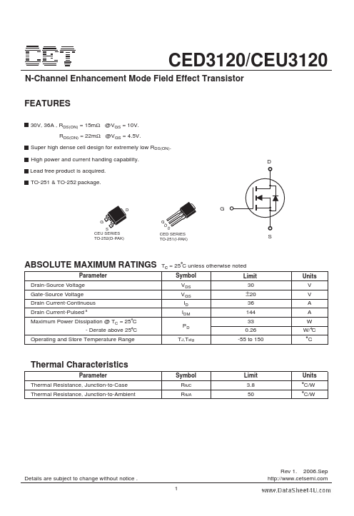
* 30V, 36A , RDS(ON) = 15mΩ @VGS = 10V. RDS(ON) = 22mΩ @VGS = 4.5V. Super high dense cell design for extremely low RDS(ON). High power and current handing capability. Lead free product is acquired. TO-251 & TO-252 package. D D G S CEU SERIES TO-252(D-PAK) G D G S CED SERIES TO-251(I-PAK) S ABSOLUT
Datasheet Details
CEU3120
CET
242.36 KB
N-channel mosfet.
CEU3120 Distributor
📁 Related Datasheet
CEU3100 N-Channel MOSFET (CET)
CEU3172 N-Channel MOSFET (CET)
CEU301J Disc Ceramic Capacitors (Mallory)
CEU3055L N-Channel Enhancement Mode Field Effect Transistor (Chino-Excel Technology)
CEU3055L3 Dual N-Channel Enhancement Mode Field Effect Transistor (Chino-Excel Technology)
CEU3055L5 N-Channel Enhancement Mode Field Effect Transistor (Chino-Excel Technology)
CEU3060 N-Channel MOSFET (Chino-Excel Technology)
CEU3070 N-Channel MOSFET (CET)