Datasheet4U.com
🌙
CEU30N08 Datasheet | CET
Part:
CEU30N08
Description:
N-Channel MOSFET
Category:
MOSFET
Manufacturer:
CET
Size:
401.62 KB
CEU30N08 Datasheet (PDF) Download
CET
CEU30N08
Key Features
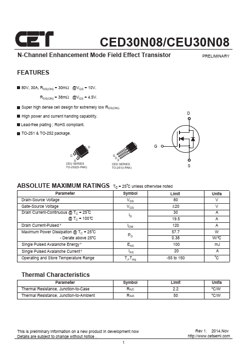
80V, 30A, RDS(ON) = 30mΩ @VGS = 10V. RDS(ON) = 38mΩ @VGS = 4.5V
×
Close