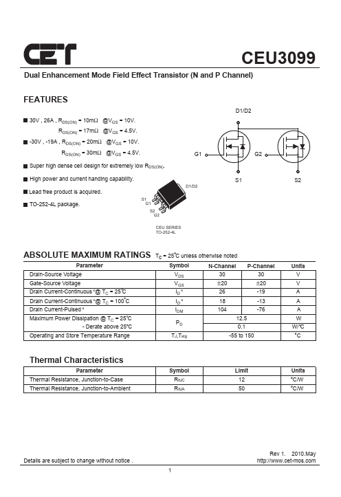
CEU3099
Dual Enhancement Mode Field Effect Transistor (N and P Channel)
FEATURES
30V , 26A , RDS(ON) = 10mΩ @VGS = 10V.
RDS(ON) = 17mΩ @VGS = 4.5V.
-30V , -19A , RDS(ON) = 20mΩ @VGS = 10V.
RDS(ON) = 30mΩ @VGS = 4.5V.
Super high dense cell design for extremely low RDS(ON).
G1
High power and current handing capability.
Lead free product is acquired.
TO-252-4L package.
S1
G1
S2
G2
D1/D2
CEU SERIES
TO-252-4L
D1/D2
G2
S1
S2
ABSOLUTE MAXIMUM RATINGS Tc = 25 C unless otherwise noted
Parameter
Symbol
N-Channel P-Channel
Drain-Source Voltage
Gate-Source Voltage
Drain Current-Continuous e@ TC = 25 C
Drain Current-Continuous e@ TC = 100 C
Drain Current-Pulsed a
Maximum Power Dissipation @ TC = 25 C
- Derate above 25 C
VDS 30 30
VGS ±20 ±20
ID e 26 -19
ID e 18 -13
IDM 104 -76
12.5
PD 0.1
Operating and Store Temperature Range
TJ,Tstg
-55 to 150
Units
V
V
A
A
A
W
W/ C
C
Thermal Characteristics
Parameter
Thermal Resistance, Junction-to-Case
Thermal Resistance, Junction-to-Ambient
Symbol
RθJC
RθJA
Limit
12
50
Units
C/W
C/W
Details are subject to change without notice .
1
Rev 1. 2010.May
http://www.cet-mos.com