CEU20P06
FEATURES
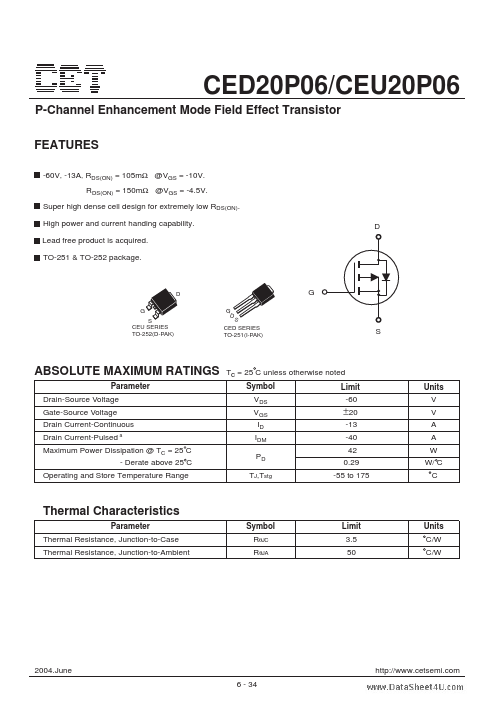
-60V, -13A, RDS(ON) = 105mΩ @VGS = -10V. RDS(ON) = 150mΩ @VGS = -4.5V. Super high dense cell design for extremely low RDS(ON). High power and current handing capability. Lead free product is acquired. TO-251 & TO-252 package. D
D G S CEU SERIES TO-252(D-PAK)
S CED SERIES TO-251(I-PAK)
ABSOLUTE MAXIMUM RATINGS
Parameter Drain-Source Voltage Gate-Source Voltage Drain Current-Continuous Drain Current-Pulsed a
Tc = 25 C unless otherwise noted Symbol Limit VDS VGS ID IDM PD TJ,Tstg -60
Units V V A A W W/ C C
±20
-13 -40 42 0.29 -55 to 175
Maximum Power Dissipation @ TC = 25 C
- Derate above 25 C Operating and Store Temperature Range
Thermal Characteristics
Parameter Thermal Resistance, Junction-to-Case Thermal Resistance, Junction-to-Ambient Symbol RθJC RθJA Limit 3.5 50 Units C/W C/W
2004.June 6
- 34 http://.cetsemi.
CED20P06/CEU20P06
Electrical Characteristics
Parameter Off Characteristics Drain-Source Breakdown Voltage Zero Gate Voltage Drain Current Gate...