CEU12N10 Overview
Key Features
- 100V, 11A, RDS(ON) = 180mΩ @VGS = 10V
- Super high dense cell design for extremely low RDS(ON)
- High power and current handing capability
- Lead free product is acquired
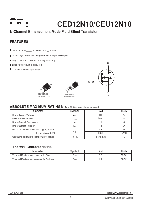
- TO-251 & TO-252 package
- D G D G S CEU SERIES TO-252(D-PAK) G D S CED SERIES TO-251(I-PAK) S