CEU04N65 Overview
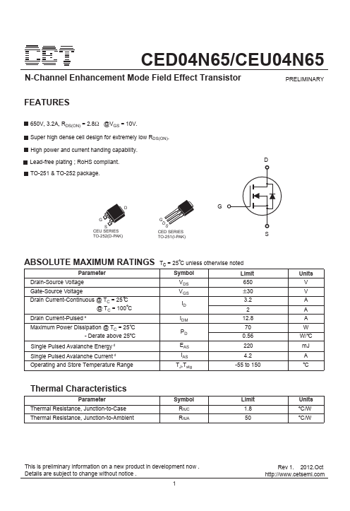
Key Features
- 650V, 3.2A, RDS(ON) = 2.8Ω @VGS = 10V
- Super high dense cell design for extremely low RDS(ON)
- High power and current handing capability
- Lead-free plating ; RoHS compliant
- TO-251 & TO-252 package
| Part | CEU04N65 |
|---|---|
| Description | N-Channel MOSFET |
| Category | MOSFET |
| Manufacturer | CET |
| Size | 378.22 KB |
| Seller | Inventory | Price Breaks | Buy |
|---|---|---|---|
| UnikeyIC | 400000 | 100+ : 0.2175 USD 200+ : 0.214 USD 300+ : 0.2085 USD |
View Offer |
| Unikeyic (ICkey) | 400000 | 100+ : 0.2175 USD 200+ : 0.214 USD 300+ : 0.2085 USD |
View Offer |
| Part Number | Manufacturer | Description |
|---|---|---|
| A2SHB | HAOHAI | N-Channel MOSFET |
| AP9563GH | Advanced Power Electronics Corp | P-CHANNEL ENHANCEMENT MODE POWER MOSFET |
| FCPF360N65S3R0L | onsemi | N-Channel MOSFET |