Datasheet4U.com
🌙
CET01N65A Datasheet | CET
Part:
CET01N65A
Description:
N-Channel MOSFET
Category:
MOSFET
Manufacturer:
CET
Size:
504.04 KB
Download CET01N65A Datasheet PDF
CET
CET01N65A
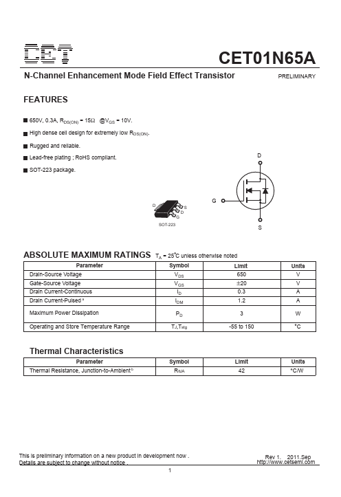
Key Features
High dense cell design for extremely low RDS(ON)
Rugged and reliable
Lead-free plating ; RoHS pliant
D DS D G SOT-223 G S
×
Close