The following content is an automatically extracted verbatim text
from the original manufacturer datasheet and is provided for reference purposes only.
View original datasheet text
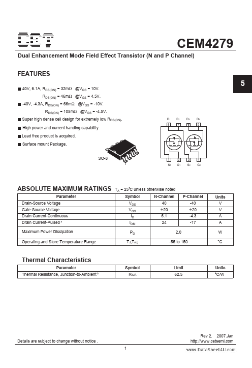
Dual Enhancement Mode Field Effect Transistor (N and P Channel)
CEM4279
5
FEATURES
40V, 6.1A, RDS(ON) = 32mΩ @VGS = 10V. RDS(ON) = 46mΩ @VGS = 4.5V. -40V, -4.3A, RDS(ON) = 66mΩ @VGS = -10V. RDS(ON) = 105mΩ @VGS = -4.5V. Super high dense cell design for extremely low RDS(ON). High power and current handing capability. Lead free product is acquired. Surface mount Package. SO-8
D1 8 D1 7 D2 6 D2 5
1
1 S1
2 G1
3 S2
4 G2
ABSOLUTE MAXIMUM RATINGS
Parameter Drain-Source Voltage Gate-Source Voltage Drain Current-Continuous Drain Current-Pulsed
a
TA = 25 C unless otherwise noted Symbol VDS VGS ID IDM PD TJ,Tstg N-Channel 40 P-Channel -40 Units V V A A W C
±20
6.1 24 2.0 -55 to 150
±20
-4.
 CEM4279 Datasheet