The following content is an automatically extracted verbatim text
from the original manufacturer datasheet and is provided for reference purposes only.
View original datasheet text
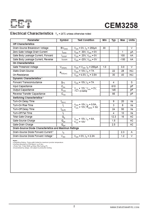
Dual N-Channel Enhancement Mode Field Effect Transistor FEATURES
30V, 7A, RDS(ON) = 28mΩ @VGS = 10V. RDS(ON) = 40mΩ @VGS = 4.5V. Super high dense cell design for extremely low RDS(ON). High power and current handing capability. Lead free product is acquired. Surface mount Package.
D1 8 D1 7
CEM3258
5
D2 6
D2 5
SO-8 1
1 S1
2 G1
3 S2
4 G2
ABSOLUTE MAXIMUM RATINGS
Parameter Drain-Source Voltage Gate-Source Voltage Drain Current-Continuous Drain Current-Pulsed
a
TA = 25 C unless otherwise noted Symbol VDS VGS ID IDM PD TJ,Tstg Limit 30 Units V V A A W C
±20
7 28 2.0 -55 to 150
Maximum Power Dissipation Operating and Store Temperature Range
Thermal Characteristics
Parameter Thermal Resistance, Junction-to-Ambient b Symbol RθJA Limit 62.
 CEM3258 Datasheet