The following content is an automatically extracted verbatim text
from the original manufacturer datasheet and is provided for reference purposes only.
View original datasheet text
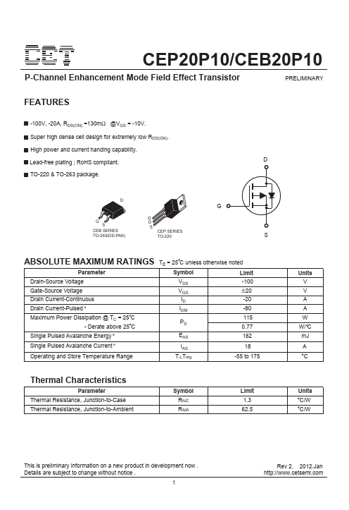
CEP20P10/CEB20P10
P-Channel Enhancement Mode Field Effect Transistor
PRELIMINARY
FEATURES
-100V, -20A, RDS(ON) =130mΩ @VGS = -10V. Super high dense cell design for extremely low RDS(ON). High power and current handing capability. Lead-free plating ; RoHS compliant. TO-220 & TO-263 package.
D
D
G S
CEB SERIES TO-263(DD-PAK)
G D S
CEP SERIES TO-220
G
S
ABSOLUTE MAXIMUM RATINGS Tc = 25 C unless otherwise noted
Parameter
Symbol
Limit
Drain-Source Voltage Gate-Source Voltage Drain Current-Continuous Drain Current-Pulsed a Maximum Power Dissipation @ TC = 25 C
- Derate above 25 C
VDS VGS ID IDM
PD
-100
±20
-20 -80 115
0.
 CEB20P10 Datasheet