Description
The THC63LVDF84C receiver supports wide temperature range as -40 to +85C, and wide frequency range as 8 to 112MHz.
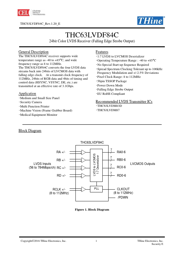
The THC63LVDF84C converts the four LVDS data streams back into 24bits of LVCMOS data with falling edge clock.
Features
- ・1:7 LVDS to LVCMOS Deserializer ・Operating Temperature Range : -40 to +85C ・No Special Start-up Sequence Required ・Spread Spectrum Clocking Tolerant up to 100kHz
Frequency Modulation and +/-2.5% Deviations ・Pixel Clock Range: 8 to 112MHz ・56pin TSSOP Package ・Power Down Mode ・Falling Edge Strobe Output ・EU RoHS Compliant
Recommended LVDS Transmitter ICs
・THC63LVDM83D ・THC63LVDM87
Block Diagram
RA +/RB +/LVDS Inputs (56 to 784Mbps/ch) RC +/RD +/-
THC63LVDF84C
LVDS to LVCMOS 1:7 Deserializer.
 THC63LVDF84C Datasheet