Continental Device India Limited
An IS/ISO 9002 and IECQ Certified Manufacturer
NPN COMPLEMENTARY SILICON HIGH VOLTAGE TRANSISTOR
IS/ISO 9002
Lic# QSC/L- 000019.2
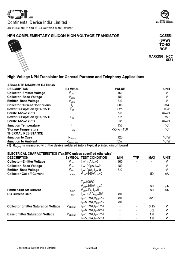
CC5551
(9AW)
TO-92
BCE
MARKING : NCC
5551
High Voltage NPN Transistor for General Purpose and Telephony Applications
ABSOLUTE MAXIMUM RATINGS
DESCRIPTION
SYMBOL
VALUE
Collector -Emitter Voltage
Collector -Base Voltage
Emitter -Base Voltage
Collector Current Continuous
Power Dissipation @Ta=25°C
Derate Above 25°C
VCEO
VCBO
VEBO
IC
PD
160
180
6.0
600
625
5.0
Power Dissipation @Tc=25°C
Derate Above 25°C
PD
1.5
12
Junction Temperature
Storage Temperature
THERMAL RESISTANCE
Tj
Tstg
150
-55 to +150
Junction to Case
Rth(j-c)
125
Junction to Ambient
Rth(j-a) (1)
357
(1) Rth(j-a) is measured with the device soldered into a typical printed circuit board
ELECTRICAL CHARACTERISTICS (Ta=25°C unless specified otherwise)
DESCRIPTION
SYMBOL TEST CONDITION
Collector -Emitter Voltage
Collector -Base Voltage
Emitter -Base Voltage
Collector-Cut off Current
VCEO
VCBO
VEBO
ICBO
IC=1mA,IB=0
IC=100µA.IE=0
IE=10µA, IC=-0
VCB=160V, IE=0
MIN
160
180
6.0
-
TYP
-
-
-
-
MAX
-
-
-
50
Ta=100°C
VCB=160V, IE=0
- - 50
Emitter-Cut off Current
IEBO VEB=4V, IC=0
- - 50
DC Current Gain
hFE* IC=1mA,VCE=5V
80 -
-
IC=10mA,VCE=5V 80 - 320
IC=50mA,VCE=5V 30 -
-
Collector Emitter Saturation Voltage VCE(Sat) * IC=10mA,IB=1mA - - 0.15
IC=50mA,IB=5mA - - 0.2
Base Emitter Saturation Voltage
VBE(Sat) * IC=10mA,IB=1mA
-
- 1.0
IC=50mA,IB=5mA - - 1.0
UNIT
V
V
V
mA
mW
mw/°C
W
mw/°C
°C
°C
°C/W
°C/W
UNIT
V
V
V
nA
µA
nA
V
V
V
V
Continental Device India Limited
Data Sheet
Page 1 of 4