The following content is an automatically extracted verbatim text
from the original manufacturer datasheet and is provided for reference purposes only.
View original datasheet text
Continental Device India Limited
An ISO/TS 16949, ISO 9001 and ISO 14001 Certified Company
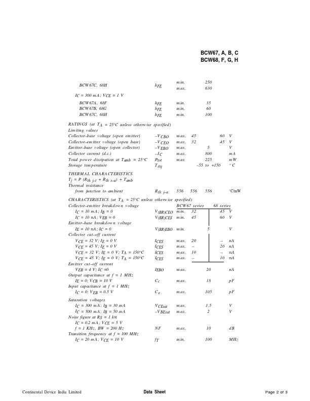
SOT-23 Formed SMD Package
BCW67, A, B, C BCW68, F, G, H
GENERAL PURPOSE TRANSISTOR
P–N–P transistor
Marking BCW67A = DA BCW67B = DB BCW67C = DC BCW68F = DF BCW68G = DG BCW68H = DH
PACKAGE OUTLINE DETAILS ALL DIMENSIONS IN mm
Pin configuration 1 = BASE 2 = EMITTER 3 = COLLECTOR
3
1
2
ABSOLUTE MAXIMUM RATINGS Collector–base voltage (open emitter) Collector–emitter voltage (open base) Emitter–base voltage (open collector) Collector current (d.c.) Total power dissipation at Tamb = 25°C D.C. current gain
IC = 10 mA; VCE = 1 V BCW67A, 68F BCW67B, 68G BCW67C, 68H
IC = 100 mA; VCE = 1 V
BCW67A, 68F
BCW67B, 68G
–VCBO –VCEO –VEBO –IC Ptot hFE hFE hFE hFE hFE
BCW 67series 68 series
max. 45
60 V
max.
 BCW67C Datasheet