Part number:
ADS8322, ADS8322_Burr
Manufacturer:
Burr-Brown Corporation
File Size:
202.40 KB
Description:
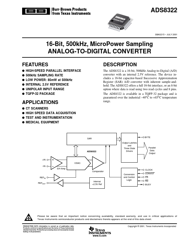
16-bit/ 500khz/ micropower sampling analog-to-digital converter.
Note:
This datasheet PDF includes multiple part numbers: ADS8322, ADS8322_Burr.
Please refer to the document for exact specifications by model.