Datasheet4U Logo Datasheet4U.com

ADS5270 - 8-Channel 12-Bit 40MSPS ADC

Download the ADS5270 datasheet PDF. This datasheet also covers the ADS5270_Burr variant, as both devices belong to the same 8-channel 12-bit 40msps adc family and are provided as variant models within a single manufacturer datasheet.

Description

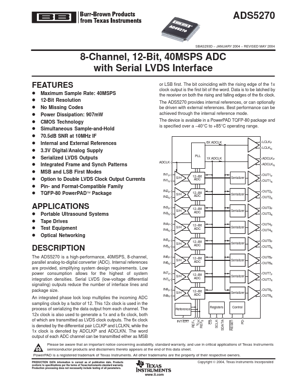
The ADS5270 is a high-performance, 40MSPS, 8-channel, parallel analog-to-digital converter (ADC).

Internal references are provided, simplifying system design requirements.

Low power consumption allows for the highest of system integration densities.

Features

  • D D D D D D D D D D D D D D D D D D D Maximum Sample Rate: 40MSPS 12-Bit Resolution No Missing Codes Power Dissipation: 907mW CMOS Technology Simultaneous Sample-and-Hold 70.5dB SNR at 10MHz IF Internal and External References 3.3V Digital/Analog Supply Serialized LVDS Outputs Integrated Frame and Synch Patterns MSB and LSB First Modes Option to Double LVDS Clock Output Currents Pin- and Format-Compatible Family TQFP-80 PowerPAD Package or LSB first. The bit coinciding with the rising edge of t.

📥 Download Datasheet

Note: The manufacturer provides a single datasheet file (ADS5270_Burr-BrownCorporation.pdf) that lists specifications for multiple related part numbers.

Full PDF Text Transcription (Reference)

The following content is an automatically extracted verbatim text from the original manufacturer datasheet and is provided for reference purposes only.

View original datasheet text
ADS5270 SBAS293D − JANUARY 2004 − REVISED MAY 2004 8-Channel, 12-Bit, 40MSPS ADC with Serial LVDS Interface FEATURES D D D D D D D D D D D D D D D D D D D Maximum Sample Rate: 40MSPS 12-Bit Resolution No Missing Codes Power Dissipation: 907mW CMOS Technology Simultaneous Sample-and-Hold 70.5dB SNR at 10MHz IF Internal and External References 3.3V Digital/Analog Supply Serialized LVDS Outputs Integrated Frame and Synch Patterns MSB and LSB First Modes Option to Double LVDS Clock Output Currents Pin- and Format-Compatible Family TQFP-80 PowerPAD Package or LSB first. The bit coinciding with the rising edge of the 1x clock output is the first bit of the word. Data is to be latched by the receiver on both the rising and falling edges of the 6x clock.
Published: |