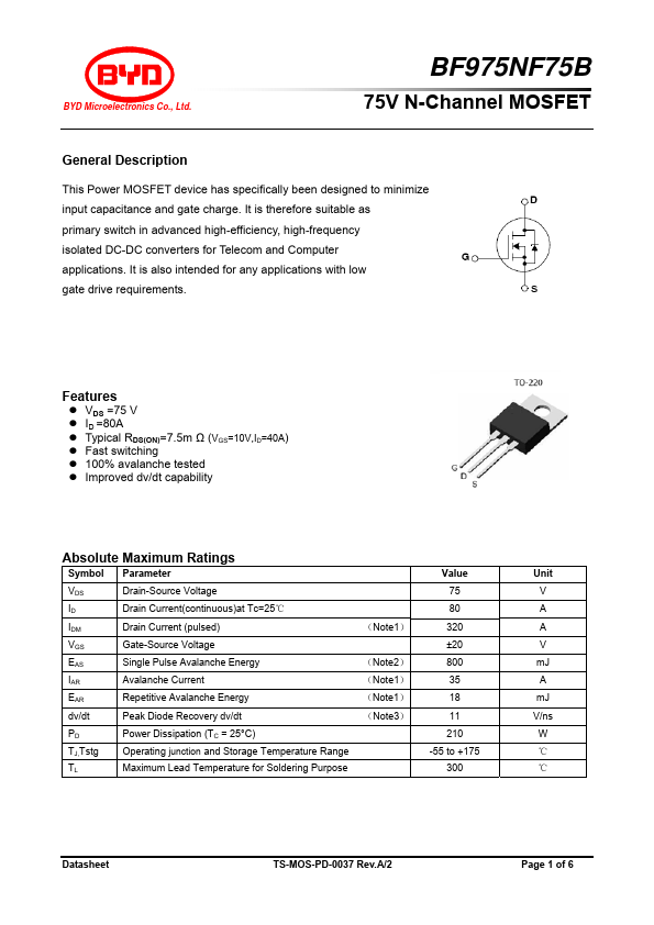
BF975NF75B
BF975NF75B is 75V N-Channel MOSFET manufactured by BYD Microelectronics.
Description
This Power MOSFET device has specifically been designed to minimize input capacitance and gate charge. It is therefore suitable as primary switch in advanced high-efficiency, high-frequency isolated DC-DC converters for Tele and puter applications. It is also intended for any applications with low gate drive requirements.
Features z z z z z z VDS =75 V ID =80A Typical RDS(ON)=7.5m Ω (VGS=10V,ID=40A) Fast switching 100% avalanche tested Improved dv/dt capability
Absolute Maximum Ratings
Symbol VDS ID IDM VGS EAS IAR EAR dv/dt PD TJ,Tstg TL Parameter Drain-Source Voltage Drain Current(continuous)at Tc=25℃ Drain Current (pulsed) Gate-Source Voltage Single Pulse Avalanche Energy Avalanche Current Repetitive Avalanche Energy Peak Diode Recovery dv/dt Power Dissipation (TC = 25°C) Operating junction and Storage Temperature Range Maximum Lead Temperature for Soldering Purpose (Note2) (Note1) (Note1) (Note3) (Note1) Value 75 80 320 ±20 800 35 18 11 210 -55 to +175 300 Unit V A A V m J A m J V/ns W ℃ ℃
TS-MOS-PD-0037 Rev.A/2
Page 1 of 6
BYD Microelectronics Co., Ltd.
Package TO-220 Packaging Tube
Ordering Information
Part Number BF975NF75B
Thermal Data
Symbol Rthj-Case Rthj-Amb Parameter Thermal Resistance Junction-Case Thermal Resistance Junction-Ambient Max. 0.6 63.0 Unit ℃/W ℃/W
Electrical Characteristics(Tc = 25℃)
Symbol V(BR)DSS IDSS IGSS VGS(th) RDS(on) Ciss Coss Crss td(on) tr td(off) tf Qg Qgs Qgd VSD(- ) Trr Parameter Drain-Source Breakdown Voltage Zero Gate Voltage Drain Current Gate-Body Leakage Current Gate Threshold Voltage Static Drain-Source On Resistance Input Capacitance Output Capacitance Reverse Transfer Capacitance Turn-On Delay Time Rise Time Turn-Off Delay Time Fall Time Total Gate Charge Gate-Source Charge Gate-Drain Charge Forward On Voltage Reverse Recovery Time ISD=25A ,VGS=0V VDD=37.5V,IF=80A,di/dt=100A/us (Note4) 70 VDD=60V, ID=80A VGS=10V (Note4, 5) VDD=37.5V, RL=15Ω VGS=10V ,RG=10Ω (Note4,5)...