Click to expand full text
*RoHS COMPLIANT
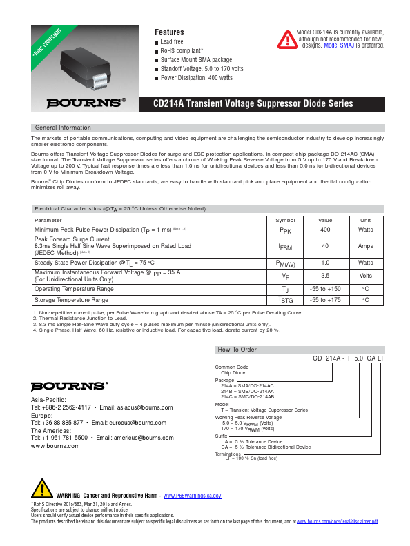
Features
Lead free RoHS compliant* Surface Mount SMA package Standoff Voltage: 5.0 to 170 volts Power Dissipation: 400 watts
Model CD214A is currently available, although not recommended for new
designs. Model SMAJ is preferred.
CD214A Transient Voltage Suppressor Diode Series
General Information
The markets of portable communications, computing and video equipment are challenging the semiconductor industry to develop increasingly smaller electronic components. Bourns offers Transient Voltage Suppressor Diodes for surge and ESD protection applications, in compact chip package DO-214AC (SMA) size format. The Transient Voltage Suppressor series offers a choice of Working Peak Reverse Voltage from 5 V up to 170 V and Breakdown Voltage up to 200 V.
 CD214A Datasheet