AX20NV2G8 Overview
................................................................................................................................. 3 Ordering Options ..................................................................................................................................... 4 Valid binations Standard......................................................................................................
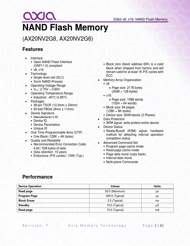
AX20NV2G8 Key Features
- Interface
- Open NAND Flash Interface (ONFI 1.0) pliant
- x8, x16
- Technology
- Single-level cell (SLC)
- 3xnm NAND Process
- Operating Voltage Range
- VCC: 2.70V
- Operating Temperature Range
- Industrial: -40°C to 85°C