AX20NV2G6
Key Features
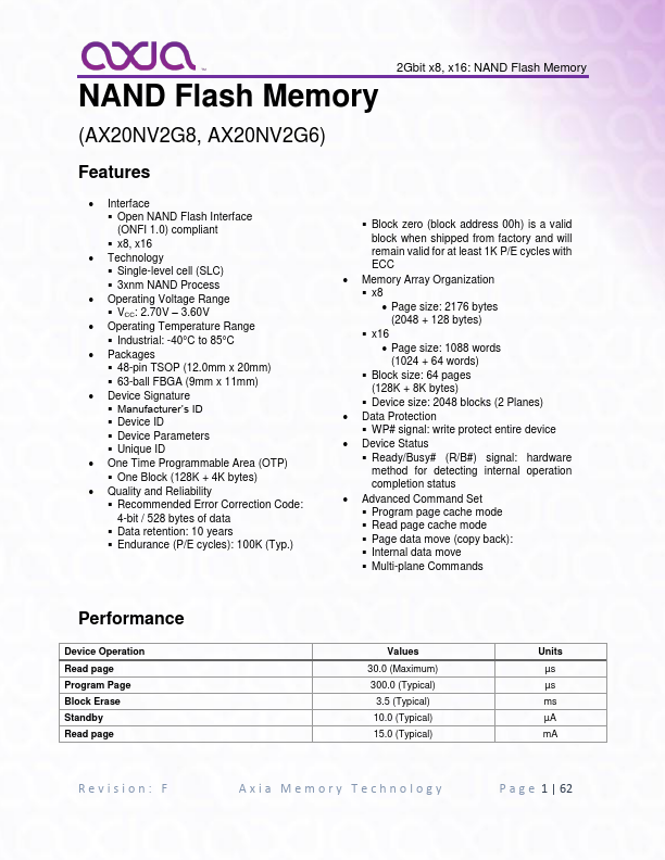
- Interface Open NAND Flash Interface (ONFI 1.0) compliant x8, x16
- Technology Single-level cell (SLC) 3xnm NAND Process
- Operating Voltage Range VCC: 2.70V – 3.60V
- Operating Temperature Range Industrial: -40°C to 85°C
- Packages 48-pin TSOP (12.0mm x 20mm) 63-ball FBGA (9mm x 11mm)
- Device Signature Manufacturer’s ID Device ID Device Parameters Unique ID
- One Time Programmable Area (OTP) One Block (128K + 4K bytes)
- Memory Array Organization x8
- Page size: 2176 bytes (2048 + 128 bytes) x16
- Page size: 1088 words (1024 + 64 words) Block size: 64 pages (128K + 8K bytes) Device size: 2048 blocks (2 Planes)