AS28F128J3A
AS28F128J3A is x8 and x16 Q-FLASH Memory manufactured by Austin Semiconductor.
FEATURES
- -
- -
- -
- -
- -
- -
- -
- -
- 100% Pin and Function patible to Intel’s MLC Family NOR Cell Architecture 2.7V to 3.6V VCC 2.7V to 3.6V or 5V VPEN (Programming Voltage) Asynchronous Page Mode Reads Manufacturer’s ID Code: 9 Numonyx 0x89h Industry Standard Pin-Out Fully patible TTL Input and Outputs mon Flash Interface [CFI] Scalable mand Set Automatic WRITE and ERASE Algorithms 5.6us per Byte effective programming time 128 bit protection register 9 64-bit unique device identifier 9 64-bit user programmable OTP cells Enhanced data protection feature with use of VPEN=VSS Security OTP block feature
100,000 ERASE cycles per BLOCK Automatic Suspend Options: 9 Block ERASE SUSPEND-to-READ 9 Block ERASE SUSPEND-to-PROGRAM 9 PROGRAM SUSPEND-to-READ Available Operating Ranges: 9 Enhanced [-ET] -40o C to +105o C 9 Mil-Temperature [-XT] -55o C to +125o C
A1 A6 A8 VPEN
AS28F128J3A Q-Flash
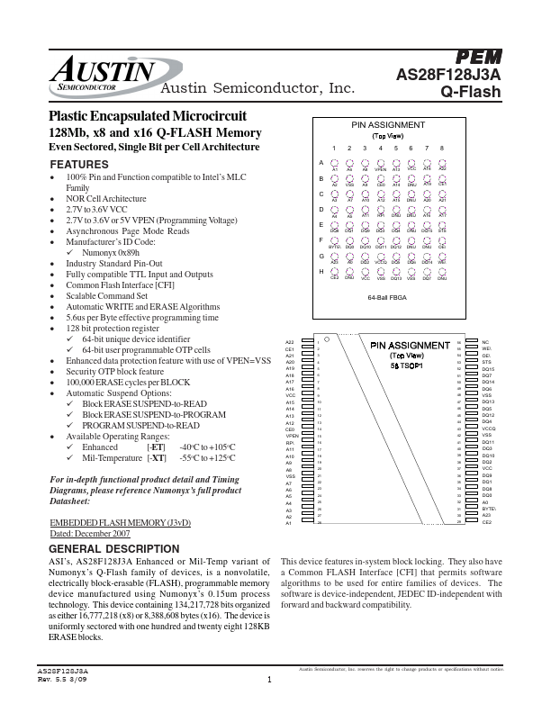
PIN ASSIGNMENT
1 2 3 4 5 6 7 8
A13
A18
A22
A2 VSS A9 CE0 A14 DNU A19 CE1
A3 A7 A10 A12 A15 DNU A20 A21
A4 A5 A11 RP DNU DNU A16 A17
DQ8 DQ1 DQ9 DQ3 DQ4 DNU DQ15 STS
BYTE DQ0 DQ10 DQ11 DQ12 DNU DNU OE
A23 A0 DQ2 VCCQ DQ5 DQ6 DQ14 WE
CE2 DNU VCC VSS DQ13 VSS DQ7 DNU
64-Ball FBGA
A22 CE1 A21 A20 A19 A18 A17 A16 VCC A15 A14 A13 A12 CE0 VPEN RP A11 A10 A9 A8 VSS A7 A6 A5 A4 A3 A2
1 2 3 4 5 6 7 8 9 10 11 12 13 14 15 16 17 18 19 20 21 22 23 24 25 26 27 28
56 55 54 53 52 51 50 49 48 47 46 45 44 43 42 41 40 39 38 37 36 35 34 33 32 31 30 29
NC WE OE STS DQ15 DQ7 DQ14 DQ6 VSS DQ13 DQ5 DQ12 DQ4 VCCQ VSS DQ11 DQ3 DQ10 DQ2 VCC DQ9 DQ1 DQ8 DQ0 A0 BYTE A23...