AT49F008AT
AT49F008AT is 8-megabit (1M x 8 / 512K x 16) Flash Memory manufactured by Atmel.
- Part of the AT49F008A comparator family.
- Part of the AT49F008A comparator family.
Features
- Single-voltage Operation
- -
- - 5V Read
- 5V Programming Fast Read Access Time
- 70 ns Internal Erase/Program Control Sector Architecture
- One 8K Word (16K Bytes) Boot Block with Programming Lockout
- Two 4K Word (8K Bytes) Parameter Blocks
- One 496K Word (992K Bytes) Main Memory Array Block Fast Sector Erase Time
- 10 seconds Byte-by-byte or Word-by-word Programming
- 10 µs Typical Hardware Data Protection Data Polling for End of Program Detection Low Power Dissipation
- 50 m A Active Current
- 100 µA CMOS Standby Current Typical 10,000 Write Cycles
- -
- -
- -
8-megabit (1M x 8/ 512K x 16) Flash Memory AT49F008A AT49F008AT AT49F8192A AT49F8192AT
Description
The AT49F008A(T) and AT49F8192A(T) are 5-volt, 8-megabit Flash memories organized as 1,048,576 words of 8 bits each or 512K words of 16 bits each. Manufactured with Atmel’s advanced nonvolatile CMOS technology, the devices offer access times to 90 ns with power dissipation of just 275 m W. When deselected, the CMOS standby current is less than 100 µA. The device contains a user-enabled “boot block” protection feature
. Two versions of the feature are available: the AT49F008A/8192A locates the boot block at lowest order addresses (“bottom boot”); the AT49F008AT/8192AT locates it at highest order addresses (“top boot”). To allow for simple in-system reprogrammability, the AT49F008A(T)/8192A(T) does not require high-input voltages for programming. Reading data out of the device is similar to reading from an EPROM; it has standard CE, OE and WE inputs to avoid bus contention. Reprogramming the AT49F008A(T)/8192A(T) is performed by first erasing a block of data and then programming on a byte-by-byte or word-by-word basis.
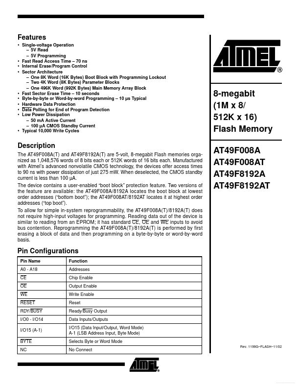
Pin Configurations
Pin Name A0
- A18 CE OE WE RESET RDY/BUSY I/O0
- I/O14 I/O15 (A-1) BYTE NC Function Addresses Chip Enable Output Enable Write Enable Reset Ready/Busy Output Data Inputs/Outputs I/O15 (Data Input/Output, Word Mode) A-1 (LSB Address Input, Byte Mode) Selects Byte or...