• Part: AZ100E111
  • Description: 1:9 Differential Clock Driver
  • Manufacturer: Arizona
  • Size: 69.63 KB
Download AZ100E111 Datasheet PDF
Arizona
AZ100E111
AZ100E111 is 1:9 Differential Clock Driver manufactured by Arizona.
.. DATA SHEET AZ10E111 AZ100E111 Features - - - - - - - - - Low Skew Guaranteed Skew Spec Differential Design Enable VBB Output Extended 100E VEE Range of -4.2V to -5.46V 75kΩ Internal Input Pulldown Resistors Direct Replacement for Motorola MC10EL111 & MC100EL111 Manufactured Under License By Lucent Technologies ARIZONA MICROTEK, INC. 1:9 Differential Clock Driver PACKAGE AVAILABILITY SUFFIX FN DESCRIPTION Plastic 28 PLCC DESCRIPTION 
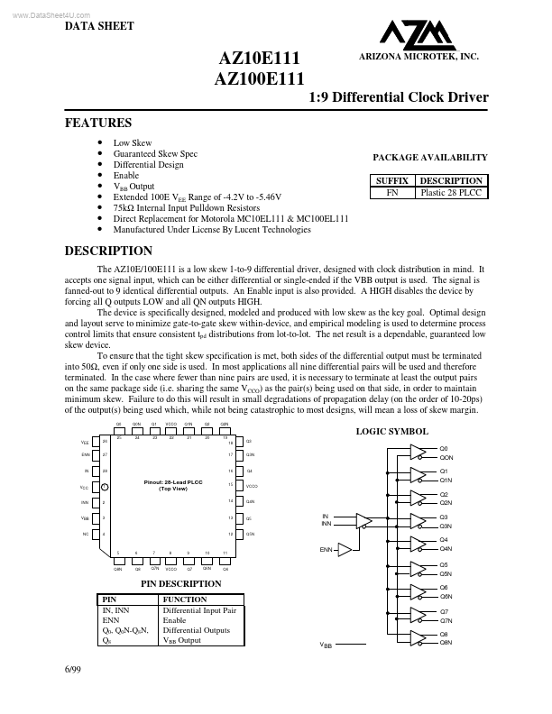
The AZ10E/100E111 is a low skew 1-to-9 differential driver, designed with clock distribution in mind. It accepts one signal input, which can be either differential or single-ended if the VBB output is used. The signal is fanned-out to 9 identical differential outputs. An Enable input is also provided. A HIGH disables the device by forcing all Q outputs LOW and all QN outputs HIGH. The device is specifically designed, modeled and produced with low skew as the key goal. Optimal design and layout serve to minimize gate-to-gate skew within-device, and empirical modeling is used to determine process control limits that ensure consistent tpd distributions from lot-to-lot. The net result is a dependable, guaranteed low skew device. To ensure that the tight skew specification is met, both sides of the differential output must be terminated into 50Ω , even if only one side is used. In most applications all nine differential pairs will be used and therefore terminated. In the case where fewer than nine pairs are used, it is necessary to terminate at least the output pairs on the same package side (i.e. sharing the same VCCO) as the pair(s) being used on that side, in order to maintain minimum skew. Failure to do this will result in small degradations of propagation delay (on the order of 10-20ps) of the output(s) being used which, while not being catastrophic to most designs, will mean a loss of skew margin. Q0 Q0N Q1 VCCO Q1N Q2 Q2N 25 VEE ENN 26 24 23 22 21 20 19 18 17 LOGIC SYMBOL Q3 Q0 27 Q3N QON Q1 Q1N Q2 Q2N IN...