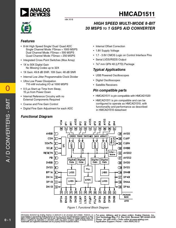
v04.1015
HMCAD1511
High Speed Multi-Mode 8-Bit
30 MSPS to 1 GSPS A/D Converter
General Description
The HMCAD1511 is a versatile high performance low power analog-to-digital converter (ADC), utilizing time-interleaving
to increase sampling rate. Integrated Cross Point Switches activate the input selected by the user.
In single channel mode, one of the four inputs can be selected as a valid input to the single ADC channel. In dual
channel mode, any two of the four inputs can be selected to each ADC channel. In quad channel mode, any input can
be assigned to any ADC channel.
An internal, low jitter and programmable clock divider makes it possible to use a single clock source for all operational
modes.
The HMCAD1511 is based on a proprietary structure, and employs internal reference circuitry, a serial control
interface and serial LVDS/RSDS output data. Data and frame synchronization clocks are supplied for data capture
at the receiver. Internal 1 to 50X digital coarse gain with ENOB > 7.5 up to 16X gain, allows digital implementation of
oscilloscope gain settings. Internal digital fine gain can be set separately for each ADC to calibrate for gain errors.
Various modes and configuration settings can be applied to the ADC through the serial control interface (SPI). Each
channel can be powered down independently and data format can be selected through this interface. A full chip idle
mode can be set by a single external pin. Register settings determine the exact function of this pin.
HMCAD1511 is designed to easily interface with Field Programmable Gate Arrays (FPGAs) from several vendors.
Electrical Specifications
DC Specifications
AVDD = 1.8V, DVDD = 1.8V, OVDD = 1.8V, FS = 125 MSPS, Quad Channel Mode, 50% clock duty cycle, -1 dBFS 70 MHz input
signal, 1x/0 dB digital gain (fine and coarse), unless otherwise noted
Parameter
DC accuracy
No missing codes
Offset
Gabs
Grel
DNL
INL
VCM,out
Analog Input
VCM,in
FSR
Cin,Q
Cin,D
Cin,S
Power Supply
VAVDD
VDVDD
VOVDD
Temperature
TA
Description
Min
Offset error after internal digital offset correction
Gain error
Gain matching between channels. ±3 sigma value at worst
case conditions
Differential non linearity
Integral non linearity
Common mode voltage output
Guaranteed
Analog input common mode voltage
Differential input voltage full scale range
Differential input capacitance, Quad channel mode
Differential input capacitance, Dual channel mode
Differential input capacitance, Single channel mode
VCM -0.1
Analog Supply Voltage
Digital and output driver supply voltage
Digital CMOS Input Supply Voltage
1.7
1.7
1.7
Operating free-air temperature
-40
Typ
0.05
±0.5
±0.2
±0.5
VAVDD/2
2
5
7
11
1.8
1.8
1.8
Max
±6
VCM +0.2
2
2
3.6
85
Unit
LSB
%FS
%FS
LSB
LSB
V
Vpp
pF
pF
pF
V
V
V
°C
0
InformationFfourrnipshreicdeb,y dAenalilvogerDye,viacensdistboelpielvaedceto obredaecrcsur:aAte naandlorgeliaDblee.vHicoewesv,erI,nnco., OFnorepTriecceh, ndoelliovegryy,Wanady,toPp.Ola.cBe ooxrd9er1s0: 6A,nNaloogrwDoeovdic,es, Inc.,
rrlTiiecgrasehpdntseosemnosfaiisbtrhkigislrirtdayannpisdtaeardrtesiegsbsuiysmttheimearedtpdmlbictyaraayAtdiorneenamsluooalrgtrkofDrstoheamevrreicwitetsihsseuefsopeurr.noidtSpsPepeurrethscyaeinofo,iycfnnatoAphetriaeopf:tinoerpsrn7retals8sinoucp1yrbeajip-cent3atcfiirvtto2ieentnong9otecw-rmShi4gnaeehu7nnrtgssp0ts.eMop0owfofAAi•ptrhnatOoa0t:uelot2nrPgdnt0shoDeot6oiecrr2venoio.ct-eheN9nes:o1r.li1n0-e68OPA0hpano0petnl-wiTAece:waNc7tiwh8Aon1n.Loa-S3Olno2ugaG9pyl-po-4WDog7ra.0tcy:0o,P•Pmh.OoOnr.deB:eo1r x-o8n90l1i0n0-e6A,aNNtAwoLrwOwwGoo.-adDn,aMloAg.0c2o0m62-9106
0-2