HMC1049LP5E
Overview
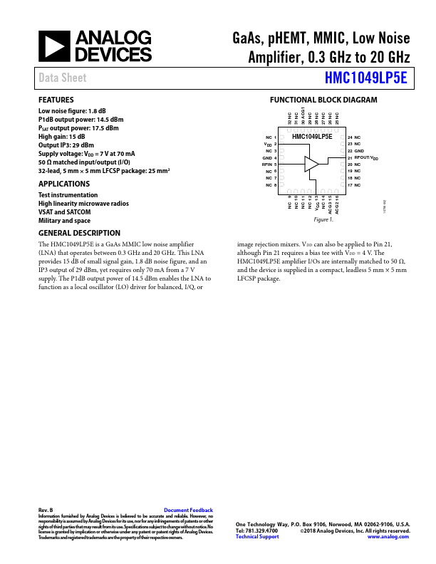
The HMC1049LP5E is a GaAs MMIC low noise amplifier (LNA) that operates between 0.3 GHz and 20 GHz. This LNA provides 15 dB of small signal gain, 1.8 dB noise.
| Part | HMC1049LP5E |
|---|---|
| Description | Low Noise Amplifier |
| Manufacturer | Analog Devices |
| Size | 325.31 KB |
The HMC1049LP5E is a GaAs MMIC low noise amplifier (LNA) that operates between 0.3 GHz and 20 GHz. This LNA provides 15 dB of small signal gain, 1.8 dB noise.
| Part Number | Manufacturer | Description |
|---|---|---|
| CS3817 | Semico | 2x15W filter-free low EMI stereo Class D audio power amplifier |
| LTK5112 | ChipSourceTek | Mono power audio amplifier |
| 4558D | New Japan Radio | DUAL OPERATIONAL AMPLIFIER |