The following content is an automatically extracted verbatim text
from the original manufacturer datasheet and is provided for reference purposes only.
View original datasheet text
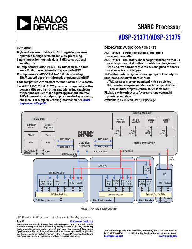
SHARC Processor ADSP-21371/ADSP-21375
SUMMARY
High performance 32-bit/40-bit floating point processor optimized for high performance audio processing
Single-instruction, multiple-data (SIMD) computational architecture
On-chip memory, ADSP-21371—1M bits of on-chip SRAM and 4M bits of on-chip mask-programmable ROM
On-chip memory, ADSP-21375—0.5M bits of on-chip SRAM and 2M bits of on-chip mask-programmable ROM
Code compatible with all other members of the SHARC family
The ADSP-21371/ADSP-21375 processors are available with a 200/266 MHz core instruction rate with unique audiocentric peripherals such as the digital applications interface, S/PDIF transceiver, serial ports, precision clock generators, and more. For complete ordering information, see Ordering Guide on Page 56.
 ADSP-21375 Datasheet