ADP5020
ADP5020 is Power Management manufactured by Analog Devices.
FEATURES
Input voltage range: 2.4 V to 5.5 V Low standby current: 1 µA Switching frequency: 3 MHz I2C interface Synchronous Buck 1 regulator: 600 m A Synchronous Buck 2 regulator: 250 m A Low dropout regulator (LDO): 150 m A Internal pensation Internal soft start Thermal shutdown 20-lead 4 mm × 4 mm LFCSP
APPLICATIONS
Digital cameras, handsets Mobile TVs
GENERAL DESCRIPTION
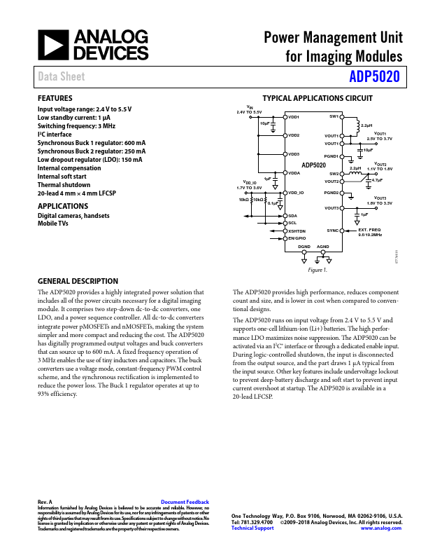
The ADP5020 provides a highly integrated power solution that includes all of the power circuits necessary for a digital imaging module. It prises two step-down dc-to-dc converters, one LDO, and a power sequence controller. All dc-to-dc converters integrate power p MOSFETs and n MOSFETs, making the system simpler and more pact and reducing the cost. The ADP5020 has digitally programmed output voltages and buck converters that can source up to 600 m A. A fixed frequency operation of 3 MHz enables the use of tiny inductors and capacitors. The buck converters use a voltage mode, constant-frequency PWM control scheme, and the synchronous rectification is implemented to reduce the power loss. The Buck 1 regulator operates at up to 93% efficiency.
Power Management Unit for Imaging Modules ADP5020
TYPICAL APPLICATIONS CIRCUIT
VIN 2.4V TO 5.5V
VDD1
SW1
10µF
2.2µH
1µF VDD_IO 1.7V TO 3.6V
10kΩ 10kΩ 0.1µF
VDD2
VOUT1 VOUT1
VDD3
PGND1
VDDA
SW2
VOUT2
VDD_IO
PGND2
SDA SCL XSHTDN EN/GPIO
VOUT3 SYNC
VOUT1 2.5V TO 3.7V 10µF
VOUT2 2.2µH 1.1V TO 1.8V
4.7µF
VOUT3 1.8V TO 3.3V 1µF
EXT. FREQ 9.6/19.2MHz
DGND AGND
07774-001
Figure 1.
The ADP5020 provides high performance, reduces ponent count and size, and is lower in cost when pared to conventional designs.
The ADP5020 runs on input voltage from 2.4 V to 5.5 V and supports one-cell lithium-ion (Li+) batteries. The high performance LDO maximizes noise suppression. The ADP5020 can be activated via an I2C® interface or through a dedicated enable input. During logic-controlled shutdown, the input is disconnected from the output source, and the...