Click to expand full text
Data Sheet
FEATURES
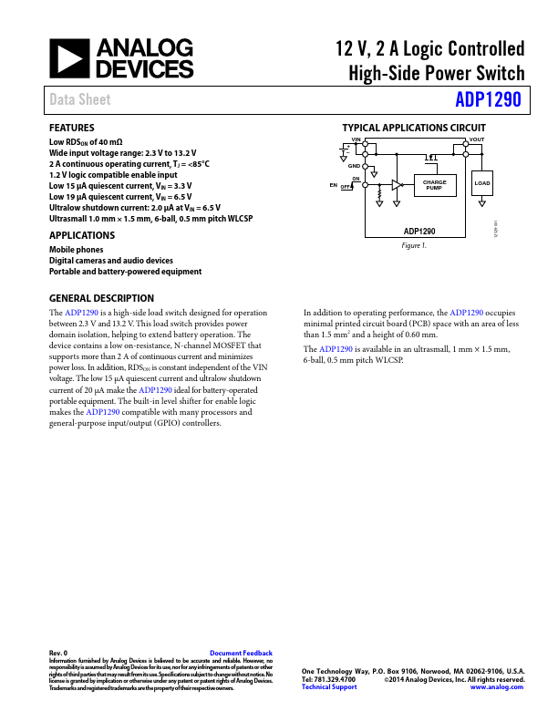
Low RDSON of 40 mΩ Wide input voltage range: 2.3 V to 13.2 V 2 A continuous operating current, TJ = <85°C 1.2 V logic compatible enable input Low 15 µA quiescent current, VIN = 3.3 V Low 19 µA quiescent current, VIN = 6.5 V Ultralow shutdown current: 2.0 µA at VIN = 6.5 V Ultrasmall 1.0 mm × 1.5 mm, 6-ball, 0.5 mm pitch WLCSP
APPLICATIONS
Mobile phones Digital cameras and audio devices Portable and battery-powered equipment
GENERAL DESCRIPTION
The ADP1290 is a high-side load switch designed for operation between 2.3 V and 13.2 V. This load switch provides power domain isolation, helping to extend battery operation. The device contains a low on-resistance, N-channel MOSFET that supports more than 2 A of continuous current and minimizes power loss.
 ADP1290 Datasheet