The following content is an automatically extracted verbatim text
from the original manufacturer datasheet and is provided for reference purposes only.
View original datasheet text
Data Sheet
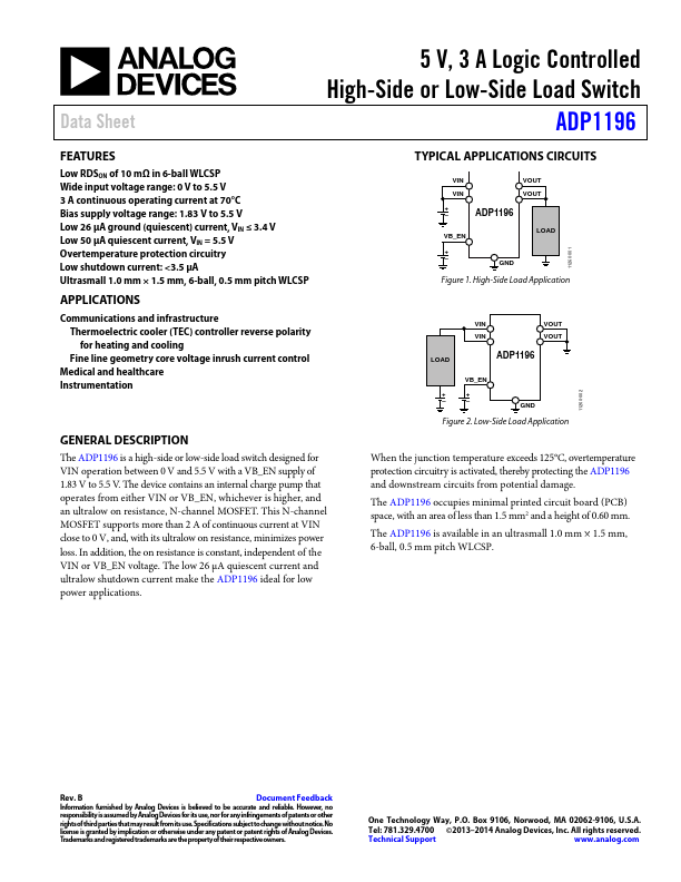
5 V, 3 A Logic Controlled High-Side or Low-Side Load Switch
ADP1196
FEATURES
Low RDSON of 10 mΩ in 6-ball WLCSP Wide input voltage range: 0 V to 5.5 V 3 A continuous operating current at 70°C Bias supply voltage range: 1.83 V to 5.5 V Low 26 µA ground (quiescent) current, VIN ≤ 3.4 V Low 50 µA quiescent current, VIN = 5.5 V Overtemperature protection circuitry Low shutdown current: <3.5 µA Ultrasmall 1.0 mm × 1.5 mm, 6-ball, 0.5 mm pitch WLCSP
APPLICATIONS
Communications and infrastructure Thermoelectric cooler (TEC) controller reverse polarity for heating and cooling Fine line geometry core voltage inrush current control
Medical and healthcare Instrumentation
GENERAL DESCRIPTION
The ADP1196 is a high-side or low-side load switch designed for VIN operation between 0 V and 5.
 ADP1196 Datasheet