Datasheet4U Logo Datasheet4U.com

ADN4665 Datasheet CMOS Differential Line Driver

Manufacturer: Analog Devices

Overview: www.DataSheet4U.com 3 V, LVDS, Quad, CMOS Differential Line Driver ADN4665 FUNCTIONAL BLOCK DIAGRAM ADN4665 DIN1 D1 DOUT1+ DOUT1– EN D4 DOUT4+ DOUT4– EN DOUT3– DOUT3+ D2 DIN2 GND.

General Description

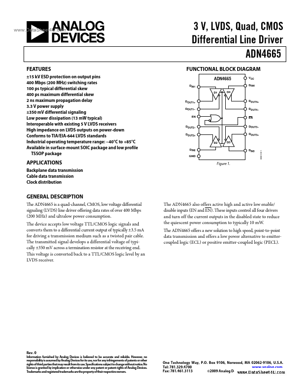
The ADN4665 is a quad-channel, CMOS, low voltage differential signaling (LVDS) line driver offering data rates of over 400 Mbps (200 MHz) and ultralow power consumption.

The device accepts low voltage TTL/CMOS logic signals and converts them to a differential current output of typically ±3.5 mA for driving a transmission medium such as a twisted pair cable.

The transmitted signal develops a differential voltage of typically ±350 mV across a termination resistor at the receiving end.

Key Features

  • ±15 kV ESD protection on output pins 400 Mbps (200 MHz) switching rates 100 ps typical differential skew 400 ps maximum differential skew 2 ns maximum propagation delay 3.3 V power supply ±350 mV differential signaling Low power dissipation (13 mW typical) Interoperable with existing 5 V LVDS receivers High impedance on LVDS outputs on power-down Conforms to TIA/EIA-644 LVDS standards Industrial operating temperature range:.
  • 40°C to +85°C Available in surface-mount SOIC package and low p.

ADN4665 Distributor & Price

Compare ADN4665 distributor prices and check real-time stock availability from major suppliers. Prices and inventory may vary by region and order quantity.