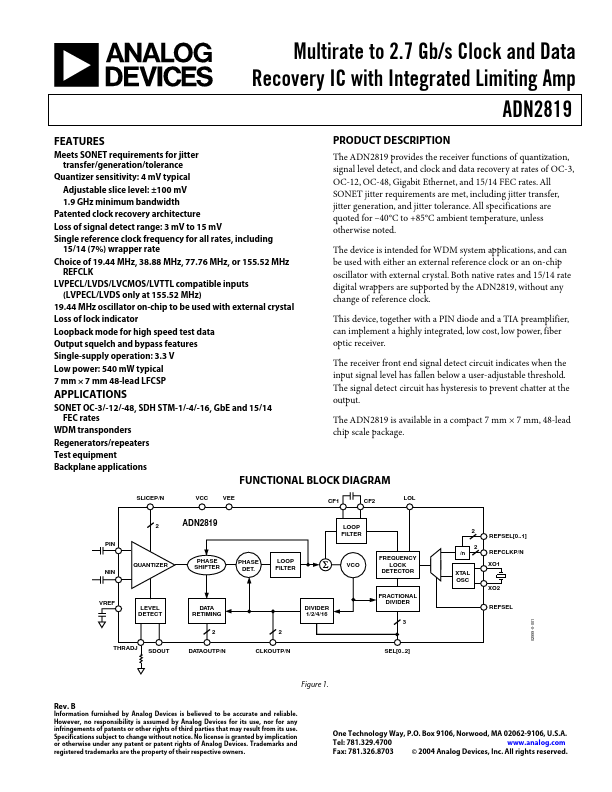
Datasheet4U Logo Datasheet4U.com

ADN2819 - Multirate to 2.7 Gb/s Clock and Data Recovery IC with Integrated Limiting Amp

Datasheet Summary

Description

The ADN2819 provides the receiver functions of quantization, signal level detect, and clock and data recovery at rates of OC-3, OC-12, OC-48, Gigabit Ethernet, and 15/14 FEC rates.

All SONET jitter requirements are met, including jitter transfer, jitter generation, and jitter tolerance.

Features

  • Meets SONET requirements for jitter transfer/generation/tolerance Quantizer sensitivity: 4 mV typical Adjustable slice level: ±100 mV 1.9 GHz minimum bandwidth Patented clock recovery architecture Loss of signal detect range: 3 mV to 15 mV Single reference clock frequency for all rates, including 15/14 (7%) wrapper rate Choice of 19.44 MHz, 38.88 MHz, 77.76 MHz, or 155.52 MHz REFCLK LVPECL/LVDS/LVCMOS/LVTTL compatible inputs (LVPECL/LVDS only at 155.52 MHz) 19.44 MHz oscillator on-chip to be use.

📥 Download Datasheet

Datasheet preview – ADN2819

Datasheet Details

Part number ADN2819
Manufacturer Analog Devices
File Size 570.28 KB
Description Multirate to 2.7 Gb/s Clock and Data Recovery IC with Integrated Limiting Amp
Datasheet download datasheet ADN2819 Datasheet
Additional preview pages of the ADN2819 datasheet.
Other Datasheets by Analog Devices

Full PDF Text Transcription

Click to expand full text
Multirate to 2.7 Gb/s Clock and Data Recovery IC with Integrated Limiting Amp ADN2819 FEATURES Meets SONET requirements for jitter transfer/generation/tolerance Quantizer sensitivity: 4 mV typical Adjustable slice level: ±100 mV 1.9 GHz minimum bandwidth Patented clock recovery architecture Loss of signal detect range: 3 mV to 15 mV Single reference clock frequency for all rates, including 15/14 (7%) wrapper rate Choice of 19.44 MHz, 38.88 MHz, 77.76 MHz, or 155.52 MHz REFCLK LVPECL/LVDS/LVCMOS/LVTTL compatible inputs (LVPECL/LVDS only at 155.52 MHz) 19.44 MHz oscillator on-chip to be used with external crystal Loss of lock indicator Loopback mode for high speed test data Output squelch and bypass features Single-supply operation: 3.
Published: |